Total cores, but going from 4 "high performance" and 4 "efficiency" to 8 "high performance" and 2 "efficiency. So should be more dramatic increase in performance than "20% more cores" would provide.
It is also important to note, despite the name with M1, we dont know if the CPU core are the same as the one used in M1 / A14. Or did they used A15 design where the energy efficient core had significant improvement. Since the Video Decoder used in M1 Pro and Max seems to be from A15, the LPDDR5 is also a new memory controller.
Going from 8 to 16 or 32 GPU cores is another massive power increase.
Prior to my current M1 MBP, my daily driver was a maxed-out 16" MBP. It's a solid computer, but it functions just as well as a space heater.
And its power adapter is only 100 watts.
The connectors never get remotely warm .. in fact under max charge rate they're consistently cool to touch, so I've always thought that it could probably be increased a little bit with no negative consequences.
It was announced earlier this year, so not in wide use yet. PDF warning: https://usb.org/sites/default/files/2021-05/USB%20PG%20USB%2...
I believe you (and Apple) that the battery can be charged faster, but I am currently rendering video on an M1 MBP. Its power draw: ~20 Watts.
That's a lot of charging overhead.
But at the same time, Apple isn't providing any hard data or explaining their methodology. I dunno how much we should be reading into the graphs. /shrug
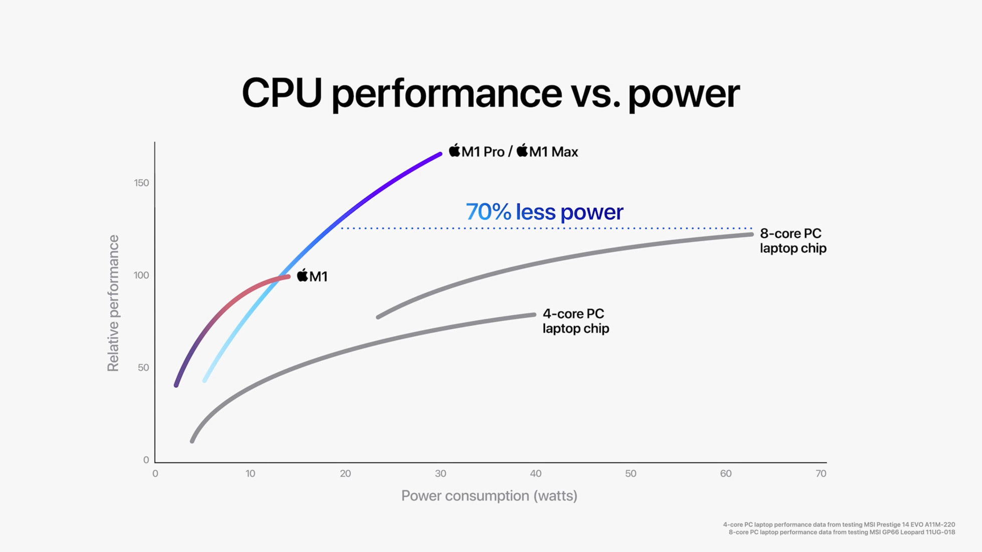
The graph there shows that the new chip is higher power usage at all performance levels.
Uses less power
https://www.apple.com/newsroom/images/product/mac/standard/A...
You'd have to be extremely old to remember that era. Lots of stuff important to making computers work got split off into separate chips away from the CPU pretty early into mass computing, such as sound, graphics, and networking. We've also been sending a lot of compute from the CPU into the GPU as late for both graphics and ML purposes.
Lately it seems like the trend has been taking these specialized peripheral chips and moving them back into SoC packages. Apple's approach here seems to be an evolutionary step on top of say, an Intel chip with integrated graphics, rather than a revolutionary step away from the era of general purpose computing.
I'm actually not sure there ever was a "true CPU computer age" where all processing was CPU-bound/CPU-based. Even the deservedly beloved MOS 6502 processor that powered everything for a hot decade or so was considered merely a "micro-controller" rather than a "micro-processor" and nearly every use of the MOS 6502 involved a lot of machine-specific video chips, memory management chips. The NES design lasted so long in part because toward then end cartridges would sometimes have entirely custom processing chips pulling work off the MOS 6502.
Even the mainframe era term itself "Central Processing Unit" has always sort of implied it always works in tandem with other "processing units", it's just the most central. (In some mainframe designs I think this was even quite literal in floorplan.) Of course too, when your CPU is a massive tower full of boards that make up individual operations and very the opposite of an Integrated Circuit, it's quite tough to call those a "general purpose CPU" as we imagine them today.
The DDR being closer to the core may or may not allow the memory to run at higher speeds due to better signal integrity, but you can purchase DDR4-5333 today whereas the M1 uses 4266.
The real advantage is the M1 Max uses 8 channels, which is impressive considering that's as many as an AMD EPYC, but operates at like twice the speed at the same time.
The step up from DDR4 to DDR5 will help fill cache misses that are predictable, but everybody uses a prefetcher already, the net effect of DDR5 is mostly just better efficiency.
The change Apple is making, moving the memory closer to the cores, improves unpredicted cache misses. That's significant.
I doubt that tRAS timing is affected by how close / far a DRAM chip is from the core. Its just a RAS command after all: transfer data from DRAM to the sense-amplifiers.
If tRAS has improved, I'd be curious how it was done. Its one of those values that's basically been constant (on a nanosecond basis) for 20 years.
Most DDR3 / DDR4 improvements have been about breaking up the chip into more-and-more groups, so that Group#1 can be issued a RAS command, then Group#2 can be issued a separate RAS command. This doesn't lower latency, it just allows the memory subsystem to parallelize the requests (increasing bandwidth but not improving the actual command latency specifically).
Has this been documented anywhere? What timings are Apple using?
They put a 32 megabyte system level cache in their latest phone chip.
>at 32MB, the new A15 dwarfs the competition’s implementations, such as the 3MB SLC on the Snapdragon 888 or the estimated 6-8MB SLC on the Exynos 2100
https://www.anandtech.com/show/16983/the-apple-a15-soc-perfo...
It will be interesting to see how big they go on these chips.
AMD's upcoming Ryzen are supposed to have 192MB L3 "v-cache" SRAM stacked above each chiplet. Current chiplets are 8-core. I'm not sure if this is a single chiplet but supposedly good for 2Tbps[1].
Slightly bigger chip than a iphone chip yes. :) But also wow a lot of cache. Having it stacked above rather than built in to the core is another game-changing move, since a) your core has more space b) you can 3D stack many layers of cache atop.
This has already been used on their GPUs, where the 6800 & 6900 have 128MB of L3 "Infinity cache" providing 1.66TBps. It's also largely how these cards get by with "only" 512GBps worth of GDDR6 feeding them (256bit/quad-channel... at 16GT). AMD's R9 Fury from spring 2015 had 1TBps of HBM2, for compare, albeit via that slow 4096bit wide interface.
Anyhow, I'm also in awe of the speed wins Apple got here from bringing RAM in close. Cache is a huge huge help. Plus 400GBps main memory is truly awesome, and it's neat that either the CPU or GPU can make use of it.
[1] https://www.anandtech.com/show/16725/amd-demonstrates-stacke...
But they're probably using 8-channels of LPDDR5, if this 400GB/s number is to be believed. Which is far more memory channels / bandwidth than any normal chip released so far, EPYC and Skylake-server included.
So its still quite unusual. Its like Apple decided to take commodity phone-RAM and just make many parallel channels of it... rather than using high-speed RAM to begin with.
HBM is specifically designed to be soldered near a CPU/GPU as well. For them to be soldering commodity LPDDR6 is kinda weird to me.
---------
We know it isn't HBM because HBM is 1024-bits at lower clock speeds. Apple is saying they have 512-bits across 8 channels (64-bits per channel), which is near LPDDR5 / DDR kind of numbers.
200GBps is within the realm of 1x HBM channel (1024-bit at low clock speeds), and 400GBps is 2x HBM channels (2048-bit bus at low clock speeds).
Also we know it's not HBM because the word "LPDDR5" was literally on the slides :)
> just make many parallel channels of it
isn't that just how LPDDR is in general? It has much narrower channels than DDR so you need much more of them?
Well yeah. But 400GBps is equivalent to 16x DDR4 channels. Its an absurdly huge amount of bandwidth.
My understanding is that bringing the RAM closer increases the bandwidth (better latency and larger buses), not necessarily the speed of the RAM dies. Also, if I am not mistaken, the RAM in the new M1s is LP-DDR5 (I read that, but it did not stay long on screen so I could be mistaken). Not sure how it is comparable with DDR4 DIMMs.
Better signal integrity could allow for larger busses, but I don't think this is actually a single 512 bit bus. I think it's multiple channels of smaller busses (32 or 64 bit). There's a big difference from an electrical design perspective (byte lane skew requirements are harder to meet when you have 64 of them). That said, I think multiple channels is better anyway.
The original M1 used LPDDR4 but I think the new ones use some form of DDR5.
I do wonder if there are nonlinearities that come in to play when it comes to these bottlenecks. Yes, by moving the RAM closer it's only reducing the latency by 0.2 ns. But, it's also taking 1/3rd of the time that it used to, and maybe they can use that extra time to do 2 or 3 transactions instead. Latency and bandwidth are inversely related, after all!
I suspect the only people who really know are the CPU manufacturer teams that run PIN/dynamorio traces against models -- and I also suspect that they are NDA'd through this life and the next and the only way we will ever know about the tradeoffs are when we see them pop up in actual designs years down the road.
I wonder about the practicalities of going to SRAM for main memory. I doubt silicon real estate would be the limiting factor (1T1C to 6T, isn't it?) and Apple charges a king's ransom for RAM anyway. Power might be a problem though. Does anyone have figures for SRAM power consumption on modern processes?
I've been wondering about this for years. Assuming the difference is similar to the old days, I'd take 2-4GB of SRAM over 32GB of DRAM any day. Last time this came up people claimed SRAM power consumption would be prohibitive, but I have a hard time seeing that given these 50B transistor chips running at several GHz. Most of the transistors in an SRAM are not switching, so they should be optimized for leakage and they'd still be way faster than DRAM.
Testing showed that the M1's performance cores had a surprising amount of memory bandwidth.
>One aspect we’ve never really had the opportunity to test is exactly how good Apple’s cores are in terms of memory bandwidth. Inside of the M1, the results are ground-breaking: A single Firestorm achieves memory reads up to around 58GB/s, with memory writes coming in at 33-36GB/s. Most importantly, memory copies land in at 60 to 62GB/s depending if you’re using scalar or vector instructions. The fact that a single Firestorm core can almost saturate the memory controllers is astounding and something we’ve never seen in a design before.
https://www.anandtech.com/show/16252/mac-mini-apple-m1-teste...
(SRAM is prohibitively expensive to do at scale due to die area required).
Edit: Nope, I'm wrong. It's pretty much only Power that has this.
IBM has eDRAM on a number of chips in varying capacities, but... its difficult for me to think of Intel, AMD, Apple, ARM, or other chips that have eDRAM of any kind.
Intel had one: the eDRAM "Crystalwell" chip, but that is seemingly a one-off and never attempted again. Even then, this was a 2nd die that was "glued" onto the main chip, and not like IBM's truly eDRAM (embedded into the same process).
EDIT: Oh, apparently there were smaller 64MB eDRAM on later chips, as you mentioned. Well, today I learned something.
Crystalwell was the codename for the eDRAM that was grafted onto Broadwell. (EDIT: Apparently Haswell, but... yeah. Crystalwell + Haswell for eDRAM goodness)
I think it's the same with Intel too except for that one 5th gen chip.
It's not just throughput that counts, but latency. Any numbers to compare there?
AVX512 suffers from bandwidth on desktop. But now the bandwidth is just huge and SVE2 is naturally scalable. Sounds like free lunch?
My 2-year-old Intel MBP has 64 GB, and 8 GB of additional memory on the GPU. True, on the M1 Max you don't have to copy back and forth between CPU and GPU thanks to integrated memory, but the new MBP still has less total memory than my 2-year-old Intel MBP.
And it seems they just barely managed to get to 64 GiB. The whole processor chip is surrounded by memory chips. That's in part why I'm curious to see how they'll scale this. One idea would be to just have several M1 Max SoCs on a board, but that's going to be interesting to program. And getting to 1 TB of memory seems infeasible too.
I guess for me I would prefer an emphasis on speed/bandwidth rather than size, but I'm also aware there are workloads that I'm completely ignorant of.
I have 32GB, so unless I’m careless everything usually fits in memory without swapping. If you got over things get slow and you notice.
I'm finding I need to commit and print a lot of these. Logic's little checker in the upper right showing RAM, Disk IO, CPU, etc also show that it is getting close to memory limits on certain instruments with many layers.
So as someone who would be willing to dump $4k into a laptop where its main workload is only audio production, I would feel much safer going with 64GB knowing there's no real upgrade if I were to go with the 32GB model outside of buying a totally new machine.
Edit: And yes, there is does show the typical "fear of committing" issue that plagues all of us people making music. It's more of a "nice to have" than a necessity, but I would still consider it a wise investment. At least in my eyes. Everyone's workflow varies and others have different opinions on the matter.
I have to wonder how Apple plans to replace the Mac Pro - the whole benefit of M1 is that gluing the memory to the chip (in a user-hostile way) provides significant performance benefits; but I don't see Apple actually engineering a 1TB+ RAM SKU or an Apple Silicon machine with socketed DRAM channels anytime soon.
My bet is that they will get rid of the Mac Pro entirely. Too low ROI for them at this point.
My hope is to see an ARM workstation where all components are standard and serviceable.
I cannot believe we are in the era of glued batteries and soldered SSDs that are guaranteed to fail and take the whole machine with them.
16-32GB of RAM on the SOC, with DRAM sockets for usage past the built in amount.
Though by the time we see an ARM MacPro they might move to stacked DRAM on the SOC. But i'd really think two tier memory system would be apple's method of choice.
I'd also expect a dual SOC setup.
So I don't expect to see that anytime soon.
I'd love to get my hands on a Mac Mini with the M1 Max.
And unused RAM isn't wasted - the system will use it for caching. Frankly I see memory as one of the cheapest performance variables you can tweak in any system.
Don't worry, Chrome will eat that up in no time!
More seriously, I look forward to more RAM for some of the datasets I work with. At least so I don't have to close everything else while running those workloads.
Some of my projects work with big in memory databases. Add regular tasks and video processing on top and there you go.
I could of course chop up the workload earlier, or use samples more often. Still, while not strictly necessary, I regularly find I get stuff done quicker and with less effort thanks to it.
But I love the fact that you have this cute little theory to doubt my actual experience to infer that I would make this up.
The facts were suspect, your follow up is further proof I had good reason to be suspect. First off, the RAW images from a 5D aren’t 16 bit. ;) Importantly, the out of memory error had nothing to do with the “16 bit RAW files”, it was video rendering lots of high res images that was the issue which is a very different issue and of course lots of RAM is needed there. Anyway, notice I said “but it’s plausible if you’ve way undersold what you’re doing”, which is definitely the case here, so I’m not sure why it bothered you.
> Canon RAW images are 14bit
You don’t see the issue?
> Are you just trying to be argumentative for the fun?
In the beginning, I very politely asked a clarifying question making sure not to call you a liar as I was sure there was more to the story. You’re the one who’s been defensive and combative since, and honestly misrepresenting facts the entire time. Where you wrong at any point? Only slightly, but you left out so many details that were actually important to the story for anyone to get any value out of your anecdata. Thanks to my persistence, anyone who wanted to learn from your experience now can.
>> I was processing 16bit RAW images at full resolution.
>> ...using After Effects to render out full frame ProRes 4444.
Those are two different applications to most of us. No one is accusing you of making things up, just that the first post wasn't fully descriptive of your use case.
Some of the genetics stuff I work on requires absolute gobs of RAM. I have a single process that requires around 400GB of RAM that I need to run quite regularly.
Isn’t that just the OS saying “unused memory is wasted memory”? Most of it is likely cache that can easily be evicted with higher memory pressure.
I mean, some of this comes down to poor executive function on my part, failing to manage resources I’m no longer using. But that’s also a valid use case for me and I’m much more effective at whatever I’m doing if I can defer it with a larger memory capacity.
You answered yourself.
Also note M1's unified memory model is actually worse for memory use not better. Details left as an exercise for the reader.
From the perspective of your GPU, that 64GB of main memory attached to your CPU is almost as slow to fetch from as if it were memory on a separate NUMA node, or even pages swapped to an NVMe disk. It may as well not be considered "memory" at all. It's effectively a secondary storage tier.
Which means that you can't really do "GPU things" (e.g. working with hugely detailed models where it's the model itself, not the textures, that take up the space) as if you had 64GB of memory. You can maybe break apart the problem, but maybe not; it all depends on the workload. (For example, you can't really run a Tensorflow model on a GPU with less memory than the model size. Making it work would be like trying to distribute a graph-database routing query across nodes — constant back-and-forth that multiplies the runtime exponentially. Even though each step is parallelizable, on the whole it's the opposite of an embarrassingly-parallel problem.)
>The SoC has access to 16GB of unified memory. This uses 4266 MT/s LPDDR4X SDRAM (synchronous DRAM) and is mounted with the SoC using a system-in-package (SiP) design. A SoC is built from a single semiconductor die whereas a SiP connects two or more semiconductor dies. SDRAM operations are synchronised to the SoC processing clock speed. Apple describes the SDRAM as a single pool of high-bandwidth, low-latency memory, allowing apps to share data between the CPU, GPU, and Neural Engine efficiently. In other words, this memory is shared between the three different compute engines and their cores. The three don't have their own individual memory resources, which would need data moved into them. This would happen when, for example, an app executing in the CPU needs graphics processing – meaning the GPU swings into action, using data in its memory. https://www.theregister.com/2020/11/19/apple_m1_high_bandwid...
These Macs are gonna be machine learning beasts.
The GP said that they already essentially have 64GB+8GB of memory in their Intel MBP; but they don't, because it's not unified, and so the GPU can't access the 64GB. So they can only load 8GB-wide models.
Whereas with the M1 Pro/Max the GPU can access the 64GB, and so can load 64GB-wide models.
that apples specific use cases for the m1 series is basically "prosumer" ?
(sorry if i'm just repeating something obvious)
Roughly 190GB per minute without sound.
Trying to do special effects on more than a few seconds of 8K video would overwhelm a 64GB system, I suspect.
[0] https://www.wired.com/1997/01/did-gates-really-say-640k-is-e...
1. The high-end SSDs in all Macs can keep up with that data rate (3GB/sec) 2. Real-time video work is virtually always performed on compressed (even losslessly compressed) streams, so the data rate to stream is less than that.
I'm saying Apple might have wanted to emphasise their more standout achievements. Such as on the CPU front, where they're likely to be well ahead for a year - competition won't catch up until AMD starts shipping 5nm Zen4 CPUs in Q3/Q4 2022.
They just throw away so much of cruft from the die like PCIE PHYs, and x86 legacy I/O with large area analog circuitry.
Redundant complex DMA, and memory controller IPs are also thrown away.
Clock, and power rails on the SoC are also probably taking less space because of more shared circuitry.
Same with self-test, debug, fusing blocks, and other small tidbits.
The seemed power efficiency when PCIE was going 1.0 2.0 3.0 ... was due to dynamic power control, and link sleep.
On top of it, they simply don't haul memory nonstop over PCIE anymore, since data going to/from GPU is simply not moving anywhere.
Moreover, it's not clear how much of a bandwidth/width does M1 max CPU interconnect/bus provide.
--------
Edit: Add common sense about HPC workloads.
There is a fundamental idea called memory-access-to-computation ratio. We can't assume a 1:0 ratio since it was doing literally nothing except copying.
Typically your program needs serious fixing if it can't achieve 1:4. (This figure comes from a CUDA course. But I think it should be similar for SIMD)
Edit: also a lot of that bandwidth is fed through cache. Locality will eliminate some orders of magnitudes of memory access, depending on the code.
https://www.anandtech.com/show/16252/mac-mini-apple-m1-teste...
If we assume that frequency is 3.2Ghz and IPC of 3 with well optimized code(which is conservative for performance cores since they are extremely wide) and count only performance cores we get 5 bytes for instruction. M1 supports 128-bit Arm Neon, so peak bandwidth usage per instruction(if I didn't miss anything) is 32 bytes.
The question is: what kind of problems are people needing that want 400GB/s bandwidth on a CPU? Well, probably none frankly. The bandwidth is for the iGPU really.
The CPU just "might as well" have it, since its a system-on-a-chip. CPUs usually don't care too much about main-memory bandwidth, because its like 50ns+ away latency (or ~200 clock ticks). So to get a CPU going in any typical capacity, you'll basically want to operate out of L1 / L2 cache.
> Oh, wait, bloody Java GC might be a use for that. (LOL, FML or both).
For example, I know you meant the GC as a joke. But if you think of it, a GC is mostly following pointer->next kind of operations, which means its mostly latency bound, not bandwidth bound. It doesn't matter that you can read 400GB/s, your CPU is going to read an 8-byte pointer, wait 50-nanoseconds for the RAM to respond, get the new value, and then read a new 8-byte pointer.
Unless you can fix memory latency (and hint, no one seems to be able to do so), you'll be only able to hit 160MB/s or so, no matter how high your theoretical bandwidth is, you get latency locked at a much lower value.
Also for me the process sounds oddly familiar to vmem table walking. There is currently a RISC-V J extension drafting group. I wonder what they can come up with.
It is needed for analytic databases, e.g. ClickHouse: https://presentations.clickhouse.com/meetup53/optimizations/
But they are demonstrating with 16 cores + 30 GB/s & 128 cores + 190 GB/s. And to my understanding they did not really mention what type of computational load did they perform. So this does not sound too ridiculous. M1 max is pairing 8 cores + 400GB/s.
Answer: you literally can't. And that's why this kind of coding style will forever be latency bound.
EDIT: Prefetching works when the address can be predicted ahead of time. For example, when your CPU-core is reading "array", then "array+8", then "array+16", you can be pretty damn sure the next thing it wants to read is "array+24", so you prefetch that. There's no need to wait for the CPU to actually issue the command for "array+24", you fetch it even before the code executes.
Now if you have "0x8009230", which points to "0x81105534", which points to "0x92FB220", good luck prefetching that sequence.
--------
Which is why servers use SMT / hyperthreading, so that the core can "switch" to another thread while waiting those 50-nanoseconds / 200-cycles or so.
Thanks for the clarifications :)
Part of the problem though, is that the object graph walk pretty quickly is non contiguous, regardless of how it's laid out in memory.
Doesn't work that well for GC but for specific workloads it can work very nicely.
I always like pointing out Knuth's dancing links algorithm for Exact-covering problems. All "links" in that algorithm are of the form "1 -> 2 -> 3 -> 4 -> 5" at algorithm start.
Then, as the algorithm "guesses" particular coverings, it turns into "1->3->4->5", or "1->4", that is, always monotonically increasing.
As such, no dynamic memory is needed ever. The linked-list is "statically" allocated at the start of the program, and always traversed in memory order.
Indeed, Knuth designed the scheme as "imagine doing malloc/free" to remove each link, but then later, "free/malloc" to undo the previous steps (because in Exact-covering backtracking, you'll try something, realize its a dead end, and need to backtrack). Instead of a malloc followed up by a later free, you "just" drop the node out of the linked list, and later reinsert it. So the malloc/free is completely redundant.
In particular: a given "guess" into an exact-covering problem can only "undo" its backtracking to the full problem scope. From there, each "guess" only removes possibilities. So you use the "maximum" amount of memory at program start, you "free" (but not really) nodes each time you try a guess, and then you "reinsert" those nodes to backtrack to the original scope of the problem.
Finally, when you realize that, you might as well put them all into order for not only simplicity, but also for speed on modern computers (prefetching and all that jazz).
Its a very specific situation but... it does happen sometimes.
Apple put 32MB of cache in their latest iPhone. 128 or even 256MB of L3 cache wouldn't surprise me at all given the power benefits.
Even simple screen refresh blending say 5 layers and outputting it to a 4k screen is 190Gbits at 144 Hz.
The copying process was never that much of a big deal, but paying for 8GB of graphics ram really is.
I don't know about that? Texture memory management in games can be quite painful. You have to consider different hardware setups and being able to keep the textures you need for a certain scene in memory (or not, in which case, texture thrashing).
Using Intel's integrated video as a way to assess the benefits of unified memory is off target. Intel had a multitude of design goals for their integrated GPU and UMA was only one aspect so it's not so easy to single that out for any shortcomings that you seem to be alluding to.
You also have an (estimated from die shots) 64 megabyte SRAM system level cache and large L2 and L1 CPU caches, but you are indeed sharing the memory bandwidth between the CPU and GPU.
I'm looking forward to these getting into the hands of testers.
They’ll still do all workloads, but are optimized for certain workloads. How is that any different than say, a Xeon or EPYC cpu designed for highly threaded (server/scientific computing) applications?
The wildcard is the actual mac pro. I suspect we aren't going to hear about mac pro until next Sept/Oct events, and super unclear what direction they are going to go. Maybe allowing config of multiple M1 max SOCs somehow working together. Seems complicated.
Agreed that it's hard to see how designing a CPU just for the Mac Pro would make any kind of economic sense but equally struggling to see what else they can do!
On the other hand, we still haven't really reached the limit for GPUs.
Notebooks also have a higher profit margin, so they sell them to those who need to upgrade now. The lower-margin systems like Mini will come later. And the Mac Pro will either die or come with the next iteration of the chips.
A more realistic question would be what good hw multisocket SMP support would look like in M1 Max or later chips, as that would be a more logical thing to build if Apple wanted this.
Accelerators/Memory are just being brought on die/package here, which has been happening for a while. Integrated memory controllers come to mind.
Not exactly. M1 CPU, GPU, and RAM were all capped in the same package. New ones appear to be more a single board soldered onto mainboard, with a discrete CPU, GPU, and RAM package each capped individually if their "internals" promo video is to be believed (and it usually is an exact representation of the shipping product) https://twitter.com/cullend/status/1450203779148783616?s=20
Suspect this is a great way for them to manage demand and various yields by having 2 CPU's (or one, if the difference between pro/ max is yield on memory bandwidth) and discrete RAM/ GPU components
M1: https://d3nevzfk7ii3be.cloudfront.net/igi/ZRQGFteQwoIVFbNn
2. If you're a ML researcher you use CUDA (which only works on NVIDIA cards), they have basically a complete software lock unless you want to spend an undefined number of X hundreds of hours fixing and troubleshooting compatibility issues.
https://blog.tensorflow.org/2020/11/accelerating-tensorflow-...
What might be more interesting is to see powerful gaming rigs built around the these chips. They could have build a kickass game console with these chips.
The AWS Graviton are Neoverse cores, which are pretty good, but clearly these Apple-only M1 cores are above-and-beyond.
---------
That being said: these M1 cores (and Neoverse cores) are missing SMT / Hyperthreading, and a few other features I'd expect in a server product. Servers are fine with the bandwidth/latency tradeoff: more (better) bandwidth but at worse (highter) latencies.
"The 21464's origins began in the mid-1990s when computer scientist Joel Emer was inspired by Dean Tullsen's research into simultaneous multithreading (SMT) at the University of Washington."
SMT / Hyperthreading has nothing to do with RISC / CISC or whatever. Its just a feature some people like or don't like.
RISC CPUs (Neoverse E1 / POWER9) can perfectly do SMT if the designers wanted.
Today's CPUs are pipelined, out-of-order, speculative, superscalar, (sometimes) SMT, SIMD, multi-core with MESI-based snooping for cohesive caches. These words actually have meaning (and in particular, describe a particular attribute of performance for modern cores).
RISC or CISC? useful for internet flamewars I guess but I've literally never been able to use either term in a technical discussion.
-------
I said what I said earlier: this M1 Pro / M1 Max, and the ARM Neoverse cores, are missing SMT, which seems to come standard on every other server-class CPU (POWER9, Intel Skylake-X, AMD EPYC).
Neoverse N1 makes up for it with absurdly high core counts, so maybe its not a big deal. Apple M1 however has very small core counts, I doubt that Apple M1 would be good in a server setting... at least not with this configuration. They'd have to change things dramatically to compete at the higher end.
Intel microcode updates added new machine opcodes to address spectre/meltdown exploits.
On a true RISC, that's not possible.
Or are you going to argue that the venerable POWER-architecture is somehow not "true RISC" ??
https://www.ibm.com/support/pages/checking-aix-protection-ag...
As all CPUs have decided that hardware-accelerated division is a good idea (and in particular: microcoded, single-instruction division makes more sense than spending a bunch of L1 cache on a series of instructions that everyone knows is "just division" and/or "modulo"), microcode just makes sense.
The "/" and "%" operators are just expected on any general purpose CPU these days.
30 years ago, RISC processors didn't implement divide or modulo. Today, all processors, even the "RISC" ones, implement it.
https://9to5mac.com/2021/10/07/linux-is-now-usable-as-a-basi...
Intel used to use "ARC" cores, but recently converted to and i486.
https://en.m.wikipedia.org/wiki/AMD_Platform_Security_Proces...
Most of the additional chip area went into more GPUs and special-purpose video codec hardware. It's "just" two more cores than the vanilla M1, and some of the efficiency cores on the M1 became performance cores. So CPU-bound things like compiling code will be "only" 20-50% faster than on the M1 MacBook. The big wins are for GPU-heavy and codec-heavy workloads.
That makes sense since that's where most users will need their performance. I'm still a bit sad that the era of "general purpose computing" where CPU can do all workloads is coming to an end.
Nevertheless, impressive chips, I'm very curious where they'll take it for the Mac Pro, and (hopefully) the iMac Pro.