Greed does. DRAM makers were antitrust busted at least 7 times on my memory in Taiwan, Korea, and USA.
They are not necessarily price fixing illegally. It's just that they all keep their production and capacity expansions closely in check to not ever let prices down.
That and in rare cases when prices are down due to unexpected decline in shipments they're all very swift to shift wafers to produce something else. Feel free to dig DRAMeXchange reports for for details.
I'm not sure how they have survived bad press, but Samsung is not a good company.
Sure, you have to sacrifice more transistors for the same capacity, but newer processes can fit more on the chip, right? I recall from computer architecture classes that the benefit of DRAM is the ability to use fewer transistors, but if transistors are cheap...
(I'm sure I'm missing something here. Power consumption / heat generation? I also never really understood why SRAM continues to be so expensive, when it seems like it would obviously benefit from smaller processes.)
So even if you were to manufacture SRAM on Intel's ultra-expensive 10 nm logic process, you'd need a massive amount of silicon for the same capacity.
[1] https://fuse.wikichip.org/wp-content/uploads/2017/12/isscc-2... [2] https://d3i71xaburhd42.cloudfront.net/f20203949a744276e338d6... [3] https://www.anandtech.com/show/13999/sk-hynix-details-its-dd...
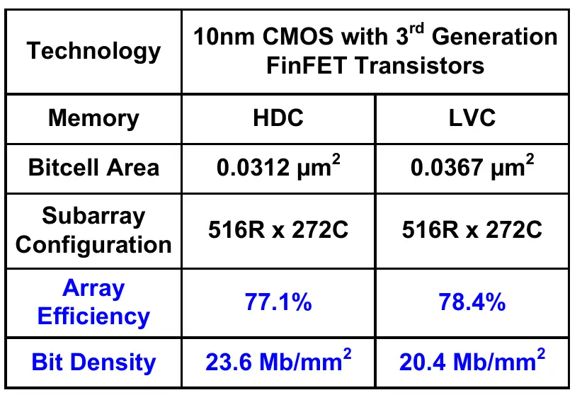

But if you have issues scaling DRAM, and different scaling limits on transistor count / SRAM, it makes sense (to me at least) to start considering SRAM as an option (e.g. for lower latency, faster speeds, higher bandwidth transfers, etc). Just because you can't achieve the same capacity today doesn't mean there's no merit to it -- HDDs vs SSDs from a decade ago feels like the obvious comparison.
Supposedly [1] TSMC's 5nm process yields 256Mb on a 5.376mm² die, at roughly ~50Mb/mm², which would translate to a 3.5Gb die of the same size as the SK Hynix chip. Sure, that's no 16Gb die, but you could easily make 32GB sticks (assuming that you could just combine these chips in the same way as in DDR4).
I guess there's also a barrier to entry in that you'd also either need new hardware to deal with "SRAM sticks", or some sort of compatibility layer (a controller that implements the DDRx signaling logic, perhaps).
[1] https://www.anandtech.com/show/15219/early-tsmc-5nm-test-chi...
Of course that all depends on the generation of tech and only applies in an apples to apples scenario.
It's really not, especially in the 3D NAND flash era where only one manufacturer is still using a floating gate cell. It's so thoroughly not transistor based that the Chinese upstart's claim to fame is that they fabricate the transistors on an entirely different wafer from the memory cells, and glue them together later.
It's best to think of NAND, DRAM and logic as three separate categories that each require a very different mix of tools in the fab, especially on the back-end. (But you won't be finding EUV or quad-patterning in the front-end of a NAND fab, either.)
Seems like RAM manufacturing is like building a casino: expensive to do, but basically a sure bet.
You could theoretically spend several times more than that to try to get ahead over the course of two or three generations, but for that kind of money you could just as easily secure some very preferential pricing from one or more of the incumbents, thereby ensuring that everyone else trying to put a lot of RAM into a PC has to pay more.
The most viable path to establishing a new leading-edge competitor in this space is for a government to throw lots of money at the problem, knowing that it'll be years at best before it produces anything competitive, but having the advantage of being able to more or less ignore IP issues and having a potential demand far higher than any one memory customer can produce on its own. China is doing this for the NAND market, too.
[0] https://www.finanznachrichten.de/nachrichten-2010-05/1694023...
that being said, I do admit my post was sarcastic, but it also did mention what the problem here is (besides a much broader discussion about captialism) which is that they can rationally expect to get away with this. State-sponsored ones because their interests are the national interest (to an extent) and privately held ones because they're usually able to effectively capture their regulators.
Also worth considering that 32TB of DRAM would draw over 12kW, just sitting there.
That's the virtual address space. A page table entry has enough bits to have a 64-bit physical address space, it just wouldn't be able to have it all mapped at once in the same virtual address space. Although CPUs don't have 64 physical address lines yet, there's nothing fundamental in the x86 architecture preventing them from doing so.
Intel have already implemented 5-level paging, which would give a 2^57 bit virtual address.
Also, this wouldn't be the first time that the x86 has supported more physical memory than virtual. PAE allowed for 64GB of RAM on a system with a 32-bit virtual address space.
While we're here I hope anyone can explain to me why Cooper Lake Xeon parts are listed as supporting 4.5TB of DDR4.
Answering self: the 4.5TB support is mostly Optane memory, not DDR4.
So the number of bits in an n-level system is 9n + 12.
9x5 + 12 = 57
On 32-bit systems the number of PT entries was 2^10, which is why they could have a 2-level system. 10x2 + 12 = 32.
IBM Power System E980, max ram: 64TB.
Expanding from 48 toward 64 bits isn't difficult.
  $ echo '(32 * 2^40) / (8 * 2^30) * 3' | bc
12288Here is the datasheet for a 128GB dimm from 2017 [1], which shows 3.4A IDD0 (normal operation) on the 1.2V rail at the highest speed of DDR4-2666, and 0.2A on the 2.5V precharge rail for a total of just over 6W. Also worth noting is that is a LRDIMM, which draws more power from the DC rails due to the additional buffering. A normal RDIMM draws a bit less static power.
Compare to a manual for a similar vintage 32GB stick [2], which consumes 2A on the 1.2V rail and 0.1A on the precharge rail for a total of a bit under 3w. One quarter the capacity, but still half of the power draw.
[1] https://www.samsung.com/semiconductor/global.semi/file/resou... [2]https://static6.arrow.com/aropdfconversion/d3b3ce1d78b0ad7d3...
Thanks for doing the math on the power story. I didn't realize about the scaling.
I thought RISC-V could with the RV128 ISA.
You should see how fast Optane will copy a project folder full of node_modules, bin, etc.. Blows the doors off an Evo Plus.
That said, probably not worth the premium for the vast majority of uses.
Not realistically; that would just introduce more problems than what I would avoid.
I have better things to do with my time than try to avoid npm.
JS projects are only a small fraction of my work anyway.
128gb dimms are more than double the price of 64gb dimms, so it not always economically viable unless you need max memory density.
Price ;=)
Also Optan drives (over PCI) are probably still interesting for some applications due to low latencies as far as I remember.
Look at base ram in MacBooks, the growth over time is pretty slow.
While both benefit greatly from economy of scale; the manufacturing tolerances, equipment, etc etc used influences pricing; but I'm not an engineer... so maybe someone here can chime in on that :)
The difference between 10µs and 60ns is merely a factor of 167 not 1 million.
The only take away I have from your comment is that you somehow confused DRAM with the L1 cache and SSDs with HDDs. That's the only way one could possibly arrive at your numbers.
I have used rounded numbers for illustrative purposes. They might be off by 30% or more but they are within the right order of magnitude.
So on 8 Channel 16 DIMM per socket you could fit a theoretical 32TB of memory. This is insane amount of memory and great for In-Memory Database. ( How is Intel Optane going to compete? )
This makes me wonder, what makes DRAM so expensive? It is still hovering at a median price or around $3/GB compared to NAND which is less than $0.1/GB.