News for hackers. Stuff that matters.
Re:DDR5 Memory Specification Released by lend000 on Thursday July 16, 2020 @04:25PM (#23863437)
The processes to form NAND and DRAM are completely different. DRAM relies on creating non-leaking capacitors which are highly difficult to manufacture at such a small scale. NAND benefits from innovations in the CPU lithography space since it's essentially all transistor based. Why would you expect them to have the same price, unless you knew nothing about the technology? Also, there are plenty of distinct competitors in the DRAM space. Do you have a source suggesting Micron and Samsung are engaging in price fixing together?
Re:DDR5 Memory Specification Released by kasabali on Thursday July 16, 2020 @05:19PM (#23863935)
"Plenty" of distinct being Samsung, Micron and Hynix.

They are not necessarily price fixing illegally. It's just that they all keep their production and capacity expansions closely in check to not ever let prices down.

That and in rare cases when prices are down due to unexpected decline in shipments they're all very swift to shift wafers to produce something else. Feel free to dig DRAMeXchange reports for for details.

Re:DDR5 Memory Specification Released by amINeolib on Thursday July 16, 2020 @10:39PM (#23866414)
Samsung is one of the worst companies. Among the BP, AT&T, Comcast, and Apple tier evils.

I'm not sure how they have survived bad press, but Samsung is not a good company.

Re:DDR5 Memory Specification Released by vitus on Thursday July 16, 2020 @07:18PM (#23865003)
If the difficulty of DRAM is in creating capacitors at that size, why haven't we seen a shift toward SRAM (6T, for instance), which is purely transistor-based?

Sure, you have to sacrifice more transistors for the same capacity, but newer processes can fit more on the chip, right? I recall from computer architecture classes that the benefit of DRAM is the ability to use fewer transistors, but if transistors are cheap...

(I'm sure I'm missing something here. Power consumption / heat generation? I also never really understood why SRAM continues to be so expensive, when it seems like it would obviously benefit from smaller processes.)

Re:DDR5 Memory Specification Released by formerly_proven on Thursday July 16, 2020 @07:49PM (#23865234)
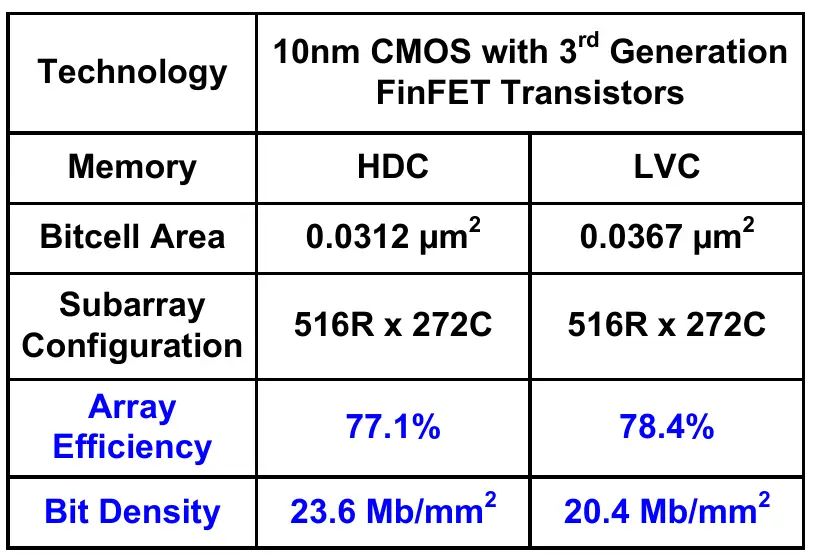
On Intel's 10 nm process you can make SRAM with a density of about 20 megabit/mm². [1] Older processes are much worse (<5 megabit/mm²). [2] A current-gen DRAM package achieves about 170 megabit/mm² (but that's two dies, probably stacked). This article [3] cites 8 Gb on 77 mm² on a 21 nm process, giving 105 megabit/mm², and 148 megabit/mm² for the DDR5 version with a die size of 54 mm². The same article shows a Samsung part with around 200 megabit/mm² density.

So even if you were to manufacture SRAM on Intel's ultra-expensive 10 nm logic process, you'd need a massive amount of silicon for the same capacity.

[1] https://fuse.wikichip.org/wp-content/uploads/2017/12/isscc-2... [2] https://d3i71xaburhd42.cloudfront.net/f20203949a744276e338d6... [3] https://www.anandtech.com/show/13999/sk-hynix-details-its-dd...
Re:DDR5 Memory Specification Released by vitus on Thursday July 16, 2020 @09:58PM (#23866173)
Totally makes sense that you wouldn't get the same capacity from the same silicon, or even close, given that SRAM uses far more transistors per cell.

But if you have issues scaling DRAM, and different scaling limits on transistor count / SRAM, it makes sense (to me at least) to start considering SRAM as an option (e.g. for lower latency, faster speeds, higher bandwidth transfers, etc). Just because you can't achieve the same capacity today doesn't mean there's no merit to it -- HDDs vs SSDs from a decade ago feels like the obvious comparison.

Supposedly [1] TSMC's 5nm process yields 256Mb on a 5.376mm² die, at roughly ~50Mb/mm², which would translate to a 3.5Gb die of the same size as the SK Hynix chip. Sure, that's no 16Gb die, but you could easily make 32GB sticks (assuming that you could just combine these chips in the same way as in DDR4).

I guess there's also a barrier to entry in that you'd also either need new hardware to deal with "SRAM sticks", or some sort of compatibility layer (a controller that implements the DDRx signaling logic, perhaps).

[1] https://www.anandtech.com/show/15219/early-tsmc-5nm-test-chi...

Re:DDR5 Memory Specification Released by g8oz on Friday July 17, 2020 @10:52AM (#23871143)
Forgive my naivete but: 20 megabit/mm^2 for SRAM...a 1u rack is 600mm X 914mm = 548,400mm^2. Multiply that by 20 megabits and that is about 70 Gigabytes. Does that mean in theory we could build a rackmount server with an external L1 cache of 70 Gigabytes? The cost would be horrendous but I'm sure there is a scenario where it could make sense.
Re:DDR5 Memory Specification Released by opwieurposiu on Friday July 17, 2020 @11:18AM (#23871452)
This would require an impractical amount of wires. For an 8 core, 64 bit cpu with differential signaling would need something like 8(64+64)2 = 2048 wires, and the length of the wires would mean the latency would be much worse then an on-die cache.
Re:DDR5 Memory Specification Released by ComputerGuru on Thursday July 16, 2020 @11:26PM (#23866663)
No, I believe SRAM actually has the edge in that department, and by a fair margin too. The d in DRAM is for dynamic as contrasted with S for static. DRAM need to be constantly read and refreshed (the timings) while SRAM doesn't and that comes with a pretty big hit to energy consumption. As soon as you add DRAM to an embedded project, the thermal/power envelop increases.

Of course that all depends on the generation of tech and only applies in an apples to apples scenario.

Re:DDR5 Memory Specification Released by wtallis on Thursday July 16, 2020 @06:12PM (#23864416)
> NAND benefits from innovations in the CPU lithography space since it's essentially all transistor based.

It's really not, especially in the 3D NAND flash era where only one manufacturer is still using a floating gate cell. It's so thoroughly not transistor based that the Chinese upstart's claim to fame is that they fabricate the transistors on an entirely different wafer from the memory cells, and glue them together later.

It's best to think of NAND, DRAM and logic as three separate categories that each require a very different mix of tools in the fab, especially on the back-end. (But you won't be finding EUV or quad-patterning in the front-end of a NAND fab, either.)