That's what your computer's power supply is: A long-lived part that delivers bulk 12V power to be regulated down to local voltages on the spot.
High performance parts will always need local voltage regulation. The VRMs must be physically close to the chip to provide a low inductance path to serve fast current transients. Moving the VRMs too far away from the chip would compromise the power delivery. Running the power through wires or connector pins is significantly worse than running through broad power planes embedded in the PCB.
At these speeds, designers spend a lot of time simulating and analyzing the power delivery network on these PCBs. The power regulation and delivery is fine tuned to support the high speeds required. You can search for "Power Delivery Network Analysis" if you want to learn more.
https://www.anandtech.com/show/16482/lenovo-thinkstation-p62...
I believe such chips can be easily unsoldered relatively easily, and reused.
And by the way, refurbished, and recycles parts, and even passives ARE a thing, it's just the part of the industry you never see in manufacturing of goods going to first world countries, but in China you can buy 2nd hand electronics components quite easily.
They do make GPUs with a socket for the asic (typically only used in test labs) so it is theoretically possible that you could for example... buy a 2070 carrier and then get nvidia to sell you a 2080 asic to socket into the carrier. But generally the technologies used in GPUs change every generation (memory technology, number of memory channels, display technologies, etc) so you probabably wouldn't be able to keep your carrier more than 1 maybe 2 generations tops.
EDIT - wait, what GPU draws 500w? I can't find one.
https://www.notebookcheck.net/The-NVIDIA-GeForce-RTX-3090-ma...
Likely no, the voltage regulation is already hard being that close to the chips and memory. A modern vrm for rtx 3090 is 16 phase by 70A stage. The gpus already have multiple power pins and with so high amps the losses in the conductor become non-trivial, hence voltage regulation is even more difficult.
Moving it farther away would make the regulation extremely conservative, overshooting and delivering too high voltage.
Even if all that happens GPUs would still require massive amounts of filtering caps.
16 phase buck controllers are greatly, greatly impractical, and the only reason the industry is stuck with them is that nobody was brave enough to do serious research into making responsive magnetic based DC-DC, while everybody knew that such thing should be possible.
It's interesting curiosity how Taiwanese made it an industry trend out of multi-phase bucks because people who were making first PCs in Taiwan had rather subpar electronics engineering education, or were basically self-taught, and designed computer boards by trial end error back in nineties.
Other than that, why would you move it to a separate part? Where? Either you push that extra cost onto the motherboard manufacturers or you need a whole new standard and slot for the VRM? What's the advantage?
These days, everything is moving towards tighter integration (fuck soldered CPUs, RAM and SSDs), so no one is going to do that.
I think the underlying premise is if you upgrade graphics cards more often or otherwise buy 2-4 graphics cards for every motherboard you buy that moving the VRM to the motherboard (and add costs there), you can still save money and reduce waste.
Those 8 pins are 12V, not 1V. They are spec'd to carry like 12.5A each - make it 15A - bit warmer wires. So around 15W per connector at 1V... and the need is over 300W. So there you have it 20 8-pin connectors.
There is a reason power lanes of the grid are higher voltage - they need a lot less current, so they are efficient. Lower voltage should remain on the PCB with multiple power planes.
Your power company does not deliver 5 volts to your house for your phone charger, nor does it transport 240 VAC more than a few parcels.
It will be, I dare you to do.
Inductance will be a problem. GPU makers are already having troubles with inductance VRM directly near the chip.
> Now, the voltage regulation is pretty darn standard.
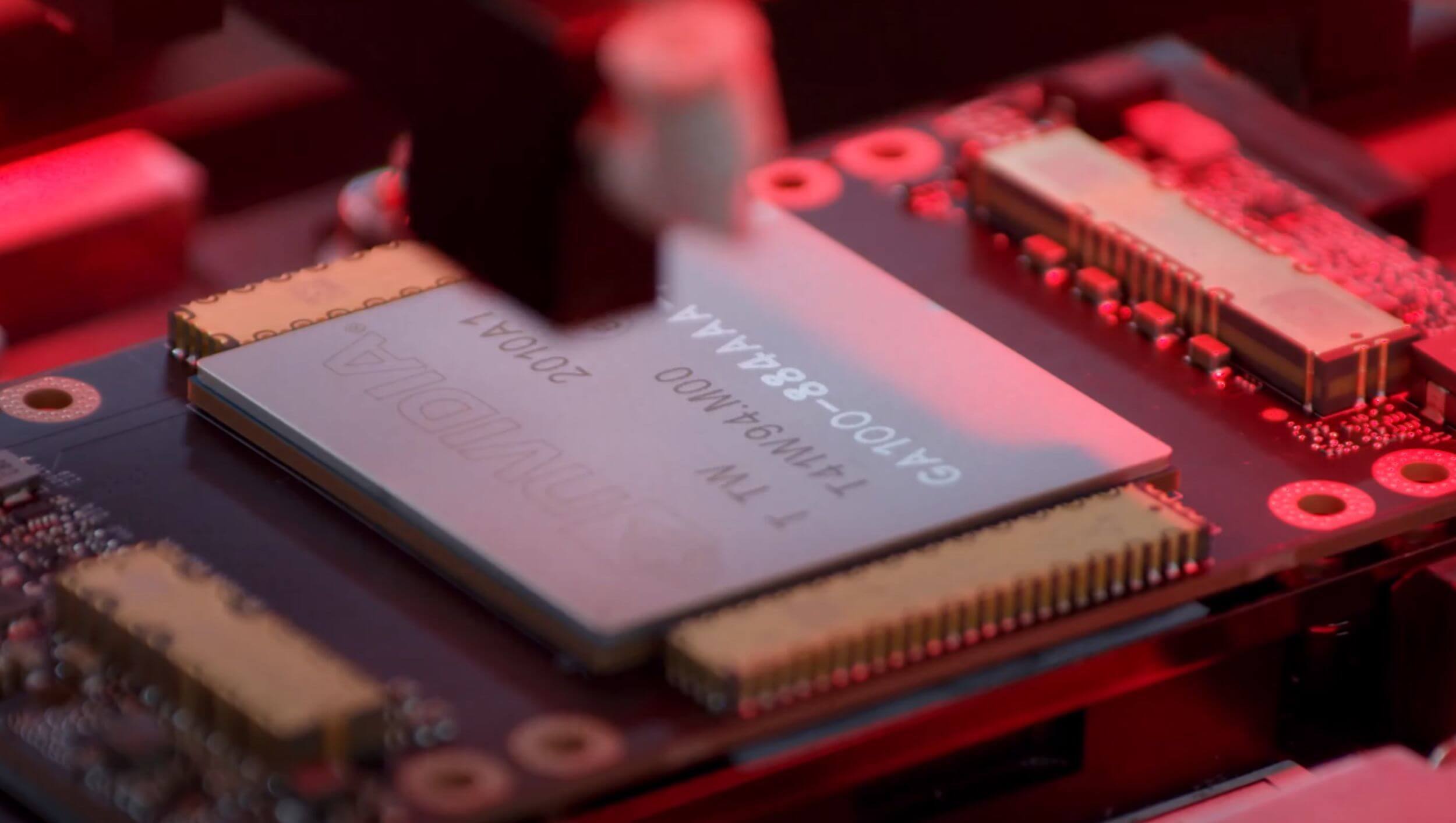
Saying this, take a look on A100
https://www.techspot.com/images2/news/bigimage/2020/05/2020-...
No VRM in a conventional sense. It's a fancy HF DC-DC with transformator!
There's a reason why monitors aren't sold as two parts: the display itself and the power circuitry.
Interestingly, it's also the one that turns off when there's some interference from the lights turning off in the next room,...
I guess I'll try re-arranging the wires if that stops the pickup of interference.
I vaguely remember it was for regulatory reasons. I searched around and it looks like it's because with an external power supply they only need to certify the brick rather than the whole unit https://www.reddit.com/r/sysadmin/comments/24jxfj/anyone_els...
It being thinner is also a bonus.
Well that's just AC/DC which is similar to the PSU of a computer or laptop. The monitor, itself, has voltage regulation for much lower volts that the one connected to the mains.
My Samsung monitor (actually a TV) does this, with any spike/dip on the mains line (eg the fridge turning on). I assumed this was just poor quality power circuitry.
Is yours a Samsung too by chance?
This way you can keep the components close to where they need to be and still get that modularity you're looking for.
But charge pumps are inefficient (like 25% efficient), take up a lot of die Space.
It would be better to have a switch mode PS generate the voltages required for erasing (effectively required for every write). On a USB key, whatever, but on a 24/7 system or laptop, it can matter.
Maybe it’s a thing now, but it’s very recent:
https://e2e.ti.com/blogs_/b/powerhouse/posts/how-to-speed-ss...
Interestingly, chips like simple USB and Ethernet controllers sometimes do feature an on-die switched-mode DC-DC circuitry to simplify the system design. You just connect an inductor and a capacitor to the DC-DC pin, and route its output to the Vcore input, pretty convenient.
The problem is transient response. The power consumption of digital processors varies wildly. For example, if a processor suddenly switches from an idle to active state, a sudden increase of current consumption makes the voltage to fall, until the regulator is able to react by conducting more power, hopefully fast and smooth enough before the processor crashes, on the scale of microseconds or even nanoseconds. This is not a trivial problem. Inductance is another problem - in any closed circuit, every piece of conductor has the tendency to resist the change of current, which means even if the regulator itself is ideal, if it's too far from the processor, it's physically impossible to react fast enough before the output voltage goes out of control, thus all ASIC requires local regulation, and the end result is extremely sensitive to board layouts and components choices.
This note describes how to build a "simulator" to test such transient currents and analyzes various circuits for this purpose - not very readable and you can just ignore this part. Just read page 1, then start reading page 6 ("Capacitor’s Role in Regulator Response") for some actual tests. Page 8 has a practical example: testing a power supply for Intel P30 Embedded Memory.
> supply tolerances are tight. Figure 26’s error budget shows only 0.1 V allowable excursion from 1.8 V, including all DC and dynamic errors. The LTC1844-1.8 regulator has a 1.75% initial tolerance (31.5 mV), leaving only a 68.5 mV dynamic error allowance.
2020 PC hardware is at least two orders of magnitude more complex than that. A simple example can be Altera Corporation AN 574: Printed Circuit Board Power Delivery Network Design Methodology for an FPGA - every single component connected to the power supply (and the circuit board itself) must be modeled and simulated as a resonant circuit with complicated frequency response and impedance characteristics [1].
[0] https://www.analog.com/media/en/technical-documentation/appl...
[1] https://www.intel.com/content/dam/www/programmable/us/en/pdf...
Now, the voltage regulation is pretty darn standard. You can chop up up half of an AMD GPU (the voltagey parts) and Frankenstein them to an NVidia GPU and have that still work [0]. The power transistors and the controllers (responsible for # of phases) are the exact same as in motherboards (they supply the CPU there).
Would it make sense to move the power delivery stuff to a separate, longer-lived part? Perhaps as part of the motherboard, or maybe have the GPU+memory+display stuff be socketable. Making a cheap 400A connector might be somewhat difficult, but not impossible.
[0] https://www.youtube.com/watch?v=4frYxrXD5Gc https://www.youtube.com/watch?v=ewkVNoMbcCc