News for hackers. Stuff that matters.
Re:Standard cells: Looking at individual gates in the Pentiu... by amelius on Sunday July 07, 2024 @02:38PM (#40899522)
Isn't modern EDA software sophiscated enough that it can place transistors as it sees fit, rather than rely on standard cells?
Re:Standard cells: Looking at individual gates in the Pentiu... by morphle on Sunday July 07, 2024 @02:59PM (#40899646)
No. Actually, the state of the art of EDA software is worse.

My project has been to design (and create) better EDA software that will simulate, optimize and therefore can form and place each individual transistor optimally to achieve lower power, higher speed and lower cost. There is only one drawback over all existing EDA software: my EDA tools must run on a ($100k) small supercomputer or FPGA cluster because it deals with a billionfold more transistors than existing EDA software and that takes more compute. It means my software is much cheaper than existing EDA software but will yield much better chips and wafers with much faster, better, cheaper and fewer transistors.

A high level overview of my software is mentioned indirectly in my talk https://vimeo.com/731037615

I'm eager to give a talk on my EDA software as well, please consider inviting me to give it?

Other researchers and companies have proven that optimizing transistor design and placement over standard cell libraries and PDKs can be done, for example:

https://www.micromagic.com/news/Ultra-Low-Power_PressRelease... was done with their own EDA software.

I am very certain (but have no hard proof) that this is what Apple did on their M1, M2 and M3 processors, especially their high end M2 Ultra chips.

What I'm claiming here is that humanity can design three to four orders of magnitude faster computer chips using at least two orders of magnitudes less energy making chips orders of magnitude cheaper if we only used better EDA software (CAD=> SYM=> FAB) that we use today. Moore's law is not at an end. I'd be happy to provide proof of this, but that takes a bit more effort than a HN comment.

Re:Standard cells: Looking at individual gates in the Pentiu... by avnd on Sunday July 07, 2024 @04:10PM (#40900108)
That’s a very ambitious project to say the least and I’ll bite! Please elaborate

Also, have you checked out the OpenROAD[1] project? It’s a pretty impressive open source RTL to GDSII flow.

I went to their most recent meetup at DAC’24 and there’s a great community around the project.

[1] https://theopenroadproject.org/

Re:Standard cells: Looking at individual gates in the Pentiu... by morphle on Sunday July 07, 2024 @05:07PM (#40900442)
>Please elaborate

I'd love to but what do you want me to elaborate on?

We started making EDA tools and simulators (CAD, SYM FAB as Alan Kay says) and designing a wafer scale integration to run parallel Squeak Smalltalk (David Ungar's ROARVM) in 2007 and we are still working on it in 2024 so I estimate 30,000 hours now. I call that very ambitious too.

>Also, have you checked out the OpenROAD[1] project? It’s a pretty impressive

No it is not pretty impressive EDA software, OpenROAD software quality is like Linux, " a budget of bad ideas" as Alan Kay typifies it. Openroad is decades old sequential program code, millions of lines of ancient C, C++ and bits of Python programs written in the very low level C language, riddled with bugs and pathes. The tools are bolted together with primitive scripts and very finicky configurations and parametric rules. Not that the commercial proprietary EDA software is any better, that usually is even worse but because you don't see the source code you can't see the underlying mess.

Good EDA tools should be written by just a few expert programmers and scientists in just a few thousand lines of code and run on a supercomputer.

So the first ambitous goal is to learn how to write better software (than the current dozens of millions of lines of EDA software code). Alan Kay explains how [1-3]:

[1] https://www.youtube.com/watch?v=ubaX1Smg6pY

[2] https://www.youtube.com/watch?v=Kj4fLRm2UC4

[3] https://www.youtube.com/watch?v=1e8VZlPBx_0

The second ambitous goal is to (learn to) design ultra low power transistor and free space optics. Learn from the best quantum physicists: [4].

https://www.youtube.com/watch?v=-dQoImLNgWs

The biggest problem is you need to get a couple of million investment just to test your software with a few tape-outs.

I only managed to invest the money for the 30,000 hours of labour so far, you can guess how many millions that's worth.

Re:Standard cells: Looking at individual gates in the Pentiu... by themoonisachees on Friday July 12, 2024 @02:49AM (#40943225)
I watched the video of your talk and it seems impressive. I work in an IP design firm, though I don't have any decision power there I could get you a foot in the door. If you're interested in trying to convince the brass, could you send an email to Eli dot senn at dolphin dot fr?
Re:Standard cells: Looking at individual gates in the Pentiu... by hansihe on Sunday July 07, 2024 @03:25PM (#40899805)
I don't know about this at any detailed level, but doesn't designing standard cells for leading edge nodes involve a lot of trial and error? Is a lot of the issues that can occur even well understood to the level that it can be simulated?

With the approach you mention, would it involve creating "custom standard cells", or would the software allow placement of every transistor outside of even a standard cell grid? If the latter, I would have trouble believing it could be feasible with the order of magnitude of computing power we have available to us today.

Re:Standard cells: Looking at individual gates in the Pentiu... by morphle on Sunday July 07, 2024 @03:32PM (#40899856)
The best results will be with custom shapes and custom individual placement of every transistor outside standard cell but within the PDK rules. Going outside the PDK rules will be even better but also harder.

The trial and error you do mostly by simulating your transistors which you than validate by making the wafers. You can simulate with mathematical models (for example in SPICE) but you should eventually try to simulate at the molecular, the atom/electron/photon and even at the quantum level, but each finer grained simulation level will take orders of magnitude more compute resources.

Chip quality is indeed limited by the magnitude of computing power and software: to design better (super)computer chips you need supercomputers.

We designed a WSI (wafer scale integration) with a million core processors and terabytes of SRAM on a wafer with 45 trillion transistors that we won't chip into chips. It would cost roughly $20K in mass production and would be the fastest cheapest desktop supercomputer to run my EDA software on so you could design even better transistors for the next step.

We also designed a $800 WSI 180nm version with 16000 cores with the same transitors as the Pentium chip in the RightTo article.

Re:Standard cells: Looking at individual gates in the Pentiu... by isotypic on Sunday July 07, 2024 @05:04PM (#40900429)
Has this WSI chip been taped out/verified? I must admit I am somewhat skeptical of TBs of SRAM, even at wafer scale integration. What would the power efficiency/cooling look like?
Re:Standard cells: Looking at individual gates in the Pentiu... by morphle on Sunday July 07, 2024 @05:11PM (#40900459)
The full WSI with 10 billion transistors at 180nm has not been taped out yet, I need $100K investment for that. This has 16K processors and a few megabyte SRAM.

I taped out 9 mm2 test chips to test transistors, the processors, programmable Morphle Logic and interconnects.

The ultra-low power 3nm WSI with trillions of transistors anda Terabyte SRAM will draw a megaWatt and would melt the transistors. So we need to simulate the transitors better and lower to power to 2 to 3 terawatt.

There is a youtube video of a teardown of the Cerebras WSI cooling system where they mention the cooling and power numbers. They also mention that they also modeled their WSI on their own supercomputer, their previous WSI.

Re:Standard cells: Looking at individual gates in the Pentiu... by initramfs on Monday July 08, 2024 @12:36AM (#40902637)
https://spectrum.ieee.org/1-bit-llm could lower power consumption of data centers.
Re:Standard cells: Looking at individual gates in the Pentiu... by Robin_Message on Monday July 08, 2024 @08:12AM (#40904682)
This sounds exciting but the enormous and confusing breadth of what your bio says you are working on, and the odd unit errors (lowering "a megawatt" to "2 to 3 terawatt), is really harming you credibility here. Do you have a link to a well-explained example of what you've achieved so far?
Re:Standard cells: Looking at individual gates in the Pentiu... by actionfromafar on Monday July 08, 2024 @10:00AM (#40905514)
Have to agree. It's fine to have past achievements in the bio I guess but if you are looking for money it doesn't hurt to appear focused.
Re:Standard cells: Looking at individual gates in the Pentiu... by osnium123 on Monday July 08, 2024 @09:56AM (#40905487)
Are you concerned that going away from standard cells will cause parametric variation, which reduces the value proposition? Have you tested your approach on leading FinFET nodes?
Re:Standard cells: Looking at individual gates in the Pentiu... by BobbyTables2 on Sunday July 07, 2024 @07:40PM (#40901410)
Could this be parallelized with a GPU?
Re:Standard cells: Looking at individual gates in the Pentiu... by morphle on Monday July 08, 2024 @12:16AM (#40902569)
I wouldn't want to do that, GPU compilers are not open source and the hardware is undocumented. As a scientist I feel they are extremely badly designed.

My transistor and atomic simulation software is extremely parallel but not in the limited SIMD way that GPU's are.

Re:Standard cells: Looking at individual gates in the Pentiu... by initramfs on Sunday July 07, 2024 @10:17PM (#40902092)
Hello, I am interested in your research as well as MicroMagics. The Claremont (32nm Pentium) and MicroMagic are the only application processors that have utilized NTV by stabilizing the voltage at 350mV-500mV. I started a project to make solar powerable mobile devices https://hackaday.io/project/177716-the-open-source-autarkic-... My email is available in the github's linked.

There are other processors, such as Ambiq Micro, but they are Cortex M4 and M55: https://www.top-electronics.com/en/apollo510-soc-250mhz-3-75...

Re:Standard cells: Looking at individual gates in the Pentiu... by morphle on Sunday July 07, 2024 @11:54PM (#40902478)
We've designed $0,10 ultra low power 8/16/32/64 bit processor SoC with built in MPPT buck/boost converters so they can be powered directly from single solar cells or small charge Li-ion cells. They have low power networking so you can create clusters. I'm not sure yet if they will be even lower power than you 5 mW processors but 1 mW is our aim.

I would argue that a solar powered computer would benefit from a 2 megabyte (could be as low as 128KB) SRAM operating system with GUI like Squeak or Smalltalk-80 instead of a Linux as you propose. We've learned a lot from the low power OLPC designs.

Thanks for the invite, I'm eager to collaborate on your solar powered computers but I'm having trouble finding your email in your githubs. Could you email us morphle73 at g mail dot com?

Re:Standard cells: Looking at individual gates in the Pentiu... by initramfs on Monday July 08, 2024 @12:31AM (#40902620)
Thanks, it is giovanni dot los___ at gmail.com (it should be in your inbox)

Also, Ambiq Micro has a 2MB MRAM (+2.75MB SRAM) processor https://www.top-electronics.com/en/apollo4-blue-plus-192-mhz... that can run on solar power (it uses ~5uA/MHz, Cortex M4) and Andreas Eriksen got LISP text editor to run on 384K RAM with the Apollo3 https://hackaday.io/project/184340-potatop and 4'4" Memory In Pixel Display.

I read that lithium-ion capacitors have much faster charging than regular li-on. https://www.tindie.com/products/jaspersikken/solar-harvestin... (and longer lifespan)

Re:Standard cells: Looking at individual gates in the Pentiu... by RF_Savage on Monday July 08, 2024 @01:53AM (#40902906)
That sounds very suitable for solar powered IoT and IIoT sensors, so the talk about GUI's feels confusing. Zephyr or freertos are perfectly fine with sub-2meg amounts if SRAM.
Re:Standard cells: Looking at individual gates in the Pentiu... by kragen on Monday July 08, 2024 @04:45AM (#40903708)
this is pretty exciting! i agree about the squeak-like approach. what would you use for the screen? i've been thinking that sharp's memory-in-pixel displays are the best option, but my power budget for the zorzpad is a milliwatt including screen, flash, and keyboard, not just the soc
Re:Standard cells: Looking at individual gates in the Pentiu... by morphle on Monday July 08, 2024 @05:40AM (#40903983)
There are ultra low power ePaper displays that only need power to change pixels but need no power to light the display or hold an image. They are usually black and white or grayscale.

> Typically, the energy required for a full switch on an E-Ink display is about 7 to 8mJ/cm2.

>The most common eInk screen takes 750 - 1800 mW during an active update

The Smalltalk-80 Alto, the Lisa and the 128K Mac had full window GUIs in black and white and desk top publishing.

The One Laptop Per Child (OLPC) had low power LCD color screens especially made for use in sunlight and would combine nicely with solar panels.

Re:Standard cells: Looking at individual gates in the Pentiu... by kragen on Monday July 08, 2024 @06:24AM (#40904153)
hey, i've been looking for those numbers for years! where did you get them?

the particular memory lcd i have is 35mm × 58mm, which is 20cm², so at 7½ millijoules per square cm, updating the same area of epaper would require 150 millijoules to update if it were epaper. the lcd in fact requires 50 microwatts to maintain the display. so, if it updates more than once every 50 minutes, it will use less power than the epaper display, by your numbers. (my previous estimate was 20 minutes, based on much less precise numbers.) at one frame per second it would use about a thousand times less power than epaper

so in this context epaper is ultra high power rather than ultra low power. and the olpc pixel qi lcds, excellent as they are, are even more power-hungry

pixel qi and epaper both have the advantage over the memory lcd that they support grayscale (and pixel qi supports color when the backlight is on)

Re:Standard cells: Looking at individual gates in the Pentiu... by morphle on Monday July 08, 2024 @04:07PM (#40909065)
>hey, i've been looking for those numbers for years! where did you get them?

I just googled "low power epaper" and read the summaries for mentions of mW and J

Re:Standard cells: Looking at individual gates in the Pentiu... by kragen on Monday July 08, 2024 @06:53PM (#40910635)
can you link to the sources that those numbers came from? i wouldn't be surprised if serp summaries were llm-generated nonsense
Re:Standard cells: Looking at individual gates in the Pentiu... by kragen on Tuesday July 09, 2024 @08:26AM (#40915270)
like, when i search for that phrase i get a lot of pages like https://www.marctech2.com/news/e-paper-faq-and-applications which is obviously llm-generated bullshit, some pages like https://goodereader.com/blog/e-paper/swedish-startup-rdot-is... with a conflicting number of 4 millijoules per square centimeter, and no links to actual sources who took measurements
Re:Standard cells: Looking at individual gates in the Pentiu... by kragen on Monday July 08, 2024 @04:41AM (#40903686)
what's ntv?
Re:Standard cells: Looking at individual gates in the Pentiu... by morphle on Monday July 08, 2024 @05:25AM (#40903918)
NTV = Near Threshold Voltage

https://www.anandtech.com/show/5555/intel-at-isscc-12-more-r...

>At IDF last year Intel's Justin Rattner demonstrated a 32nm test chip based on Intel's original Pentium architecture that could operate near its threshold voltage. The power consumption of the test chip was so low that the demo was powered by a small solar panel. A transistor's threshold voltage is the minimum voltage applied to the gate for current to flow. The logical on state is typically mapped to a voltage much higher than the threshold voltage to ensure reliable and predictable operation. The non-linear relationship between power and voltage makes operating at lower voltages, especially those near the threshold very interesting.

Re:Standard cells: Looking at individual gates in the Pentiu... by kragen on Monday July 08, 2024 @06:24AM (#40904158)
aha, thanks! the description of the threshold voltage in the text is wrong though; it would imply ambiq’s product wouldn't work at all
Re:Standard cells: Looking at individual gates in the Pentiu... by initramfs on Sunday July 07, 2024 @10:20PM (#40902102)
I read this is the software they used to make the MicroMagic https://sourceforge.net/projects/mmi-pd (someone on The Open-Source Silicon Slack mentioned it, I think https://open-source-silicon.dev/
Re:Standard cells: Looking at individual gates in the Pentiu... by anamax on Sunday July 07, 2024 @10:56PM (#40902239)
A few decades ago, Quickturn sold a custom-built FPGA cluster to do hardware simulation at the gate level.

Quickturn was bought by Cadence and now seems to be gone.

Re:Standard cells: Looking at individual gates in the Pentiu... by FastFT on Sunday July 07, 2024 @11:45PM (#40902451)
Not sure if its from Quickturn’s acquisition, but Cadence still makes a hardware simulation platform called Palladium.
Re:Standard cells: Looking at individual gates in the Pentiu... by therealcamino on Tuesday July 09, 2024 @08:08AM (#40915129)
If you have working software that gives orders of magnitude improvements, needing $100k worth of hardware would be no barrier at all. That's a fraction of just the EDA software license budget for many projects.
Re:Standard cells: Looking at individual gates in the Pentiu... by themoonisachees on Sunday July 07, 2024 @03:04PM (#40899678)
All tools at use in the last gen industry (40-12nm) currently make extensive use of standard cell librairies provided by foundries. I don't expect current gen nor next gen to change anything.

Source: I work in EDA

Re:Standard cells: Looking at individual gates in the Pentiu... by rsdfvn1099 on Monday July 08, 2024 @01:12AM (#40902772)
I definitely agree with your overall sentiment but if you actually care about your project go with one of the 3rd party standard cell libraries, i.e. https://www.synopsys.com/dw/ipdir.php?ds=dwc_standard_cell

With the foundry provided library you get what you pay for...

Re:Standard cells: Looking at individual gates in the Pentiu... by frabert on Sunday July 07, 2024 @02:46PM (#40899566)
I don't think it's a software issue -- AIUI the issue is that foundries will only let you use blocks for which the process was tested, or the yields would be unreliable/all over the place
Re:Standard cells: Looking at individual gates in the Pentiu... by quotemstr on Sunday July 07, 2024 @02:56PM (#40899631)
Really? I can't just call TSMC and say "Hey. Here's a mask. Please print 10,000, thanks."?
Re:Standard cells: Looking at individual gates in the Pentiu... by morphle on Sunday July 07, 2024 @03:02PM (#40899656)
no, the mask must be made within the tight rules of the proprietary (and very secret) PDK of the TSMC Fab for that node. Just getting it certified that it fits the rules will cost millions.

https://en.wikipedia.org/wiki/Process_design_kit

Re:Standard cells: Looking at individual gates in the Pentiu... by shrubble on Sunday July 07, 2024 @04:15PM (#40900136)
How were the Parallax Propeller guys able to do it? They have a Propeller2 that is in either 40nm or 28nm, IIRC.
Re:Standard cells: Looking at individual gates in the Pentiu... by RF_Savage on Monday July 08, 2024 @01:51AM (#40902903)
Because those are now trailing edge nodes, so cheaper and easier entry for everybody.
Re:Standard cells: Looking at individual gates in the Pentiu... by amelius on Sunday July 07, 2024 @03:04PM (#40899682)
Interesting. What is the granularity? Is it logic gates, or transistors?
Re:Standard cells: Looking at individual gates in the Pentiu... by morphle on Sunday July 07, 2024 @03:10PM (#40899719)
the granularity is at all levels: standard cells (=gates), transistor shapes, metal layer shapes down to groups of atoms (for quantum dots).
Re:Standard cells: Looking at individual gates in the Pentiu... by quotemstr on Sunday July 07, 2024 @03:03PM (#40899675)
Are all fabs like this?
Re:Standard cells: Looking at individual gates in the Pentiu... by hansihe on Sunday July 07, 2024 @03:11PM (#40899726)
It's probably more of a node thing than a fab thing. You would have a much easier time getting the fab to do random stuff for you on a legacy node compared to a leading edge node.

Leading edge nodes are basically black magic and are right on the edge of working vs producing broken chips.

You as a customer would never want to be in a position where you are solely responsible for yields.

Re:Standard cells: Looking at individual gates in the Pentiu... by morphle on Sunday July 07, 2024 @03:13PM (#40899730)
There are only a few Fabs with nodes smaller than 28nm. Yes, all fabs are like that, with exception of a few experimental tiny labs at research institutes or universities.
Re:Standard cells: Looking at individual gates in the Pentiu... by crote on Sunday July 07, 2024 @03:16PM (#40899754)
There are open-source PDKs[0] for education, research, and R&D - but they extremely rare and decades behind state-of-the-art.

Nobody wants to give away trade secrets, so everything remains proprietary and behind an NDA until it has become completely obsolete.

[0]: https://www.skywatertechnology.com/sky130-open-source-pdk/

Re:Standard cells: Looking at individual gates in the Pentiu... by amelius on Sunday July 07, 2024 @03:02PM (#40899666)
Maybe in reality it is somewhere in-between, where TSMC says: here is a set of standard cells that we tested; you can use them but if you modify anything then it's at your own risk.
Re:Standard cells: Looking at individual gates in the Pentiu... by morphle on Sunday July 07, 2024 @03:15PM (#40899745)
Maybe in therory, yes. In practise the fab will never allow you to do anything at your own risk because it might contaminate or break their $170 million machine. If you offer a few billion extra to cover that risk, your cheaper off building your own fab instead.
Re:Standard cells: Looking at individual gates in the Pentiu... by amelius on Sunday July 07, 2024 @03:23PM (#40899788)
I'm not convinced that moving transistors around freely would break the machine. How could that possibly happen?
Re:Standard cells: Looking at individual gates in the Pentiu... by haneefmubarak on Sunday July 07, 2024 @03:43PM (#40899928)
Think of it less like moving transistors around and more like moving small groups of atoms around (also, you can get single transistor cells for analog and power designs). The processes required to place the rough groups of atoms in roughly specific places involves extreme amounts of energy relative to the size of what you are working with, which is supplied in a combination of chemical, radiation, and thermal forms. As a result, predicting what additional effects attempting to form specific micro-shapes might have is nontrivial. They extensively simulate and then carefully test all of their approved cells on an ongoing basis. Deviating from this could cause unknown issues, including damage, but doing the necessary work to prequalify your custom cells would be prohibitively expensive for most applications.

NB: this is obviously a simplified explanation.

Re:Standard cells: Looking at individual gates in the Pentiu... by oasisaimlessly on Sunday July 07, 2024 @04:15PM (#40900138)
It wouldn't, except potentially for macro-level requirements like maintaining the correct fill ratio [1]. Sibling comments are FUD.

1: https://semiengineering.com/knowledge_centers/materials/fill...

Re:Standard cells: Looking at individual gates in the Pentiu... by morphle on Sunday July 07, 2024 @03:39PM (#40899905)
Going outside of the PDK rules you risk contamination because a chip machine is a high speed ultra-accurate automated mechanical and chemical laboratory. It sprays extremely corrosive acids and vaporizes metals. Going a nanometer outside of the rules would send droplet or flakes of chemicals flying around at high speed.

https://www.epfl.ch/research/facilities/cmi/equipment/photol...

Re:Standard cells: Looking at individual gates in the Pentiu... by kens on Sunday July 07, 2024 @04:36PM (#40900274)
I'm very skeptical of this too. I don't see a mechanism where moving transistors could break the machine. Although I wonder if you could blow up the die testing machine by making a chip that was one big charge pump :-)
Re:Standard cells: Looking at individual gates in the Pentiu... by rsdfvn1099 on Monday July 08, 2024 @12:59AM (#40902728)
It's not obvious what "moving" means in this thread but no foundry would ever let you make a design the grossly violates the design rule checks (DRC). It's hard to imagine how something risking damage of anything would get through all the many, many, checks, but wasting time and money is definitely possible and to be avoided.

As an aside, few analog layouts will use the "line of diffusion" style that's common in the standard cells. And in analog one can find more exotic transistor patterns, like waffle [1], that aren't used in digital. Many things are possible, but it has to pass DRC.

[1] https://www.radioeng.cz/fulltexts/2019/19_03_0598_0609.pdf

Re:Standard cells: Looking at individual gates in the Pentiu... by eternauta3k on Monday July 08, 2024 @01:16AM (#40902790)
Skeptical here as well, no one is proposing a serious mechanism for damage like "you left gate oxide uncovered by silicide so it contaminates the CMP machine" or whatever.

What I can imagine, is that the foundry only tests their magic OPC algorithm with DRC clean inputs. If your mask isn't DRC clean, who knows what's coming out the other side.

Re:Standard cells: Looking at individual gates in the Pentiu... by gary_0 on Sunday July 07, 2024 @04:41PM (#40900314)
It takes years just to figure out how to use the machines to produce actual working chips. They're the most specialized, intricate, expensive machines in the world. They're operated in enormous clean rooms that only allow for 1 half-micron sized particle per cubic foot. No fab is going to run them without exactly following the procedures they have spent billions developing and testing. They are also going to avoid potential delays as much as possible because these machines have to be running for as much of their useful life as possible to recoup the vast expense. The level of risk-averseness is insane, but warranted.

If you haven't watched this video, I highly recommend it: Indistinguishable From Magic: Manufacturing Modern Computer Chips https://www.youtube.com/watch?v=NGFhc8R_uO4 It's a little outdated now, but very comprehensive and gives you an idea of how totally nuts the chip business is.

Re:Standard cells: Looking at individual gates in the Pentiu... by anamax on Sunday July 07, 2024 @10:31PM (#40902138)
> If you offer a few billion extra to cover that risk, your cheaper off building your own fab instead.

You can't build a high-end fab for a couple of billion dollars.

Re:Standard cells: Looking at individual gates in the Pentiu... by SuperscalarMeme on Sunday July 07, 2024 @06:03PM (#40900824)
I'll give you an alternate take: the compute power available to EDA software has been roughly scaling at the same rate as transistors on a die. So the complexity of the problem relative to compute power available has remained somewhat constant. So standard cell design remains an efficient method of reducing complexity of the problems EDA tools have to solve.
Re:Standard cells: Looking at individual gates in the Pentiu... by kens on Sunday July 07, 2024 @08:47PM (#40901711)
That's an interesting thought. However, it assumes that the problem scales with the number of transistors, i.e. O(N). I expect that the complexity of place and route algorithms is worse than O(N), which means the algorithms will fall behind as the number of transistors increases. (Technically, the algorithms are NP-complete so you're doomed, but what matters is the complexity of the heuristics.)
Re:Standard cells: Looking at individual gates in the Pentiu... by morsch on Monday July 08, 2024 @01:58AM (#40902916)
It's worse than that, isn't it? Not only are the algorithms presumably super linear, the transistor count has been increasing exponentially, but the compute power per transistor has been decreasing over time. See e.g. [1].

Although I suppose if the problem is embarrassingly parallel, the SpecINT x #cores curves might just about reach the #transistors curve.

[1] https://substackcdn.com/image/fetch/w_1272,c_limit,f_webp,q_... via https://www.semianalysis.com/p/a-century-of-moores-law figure 1
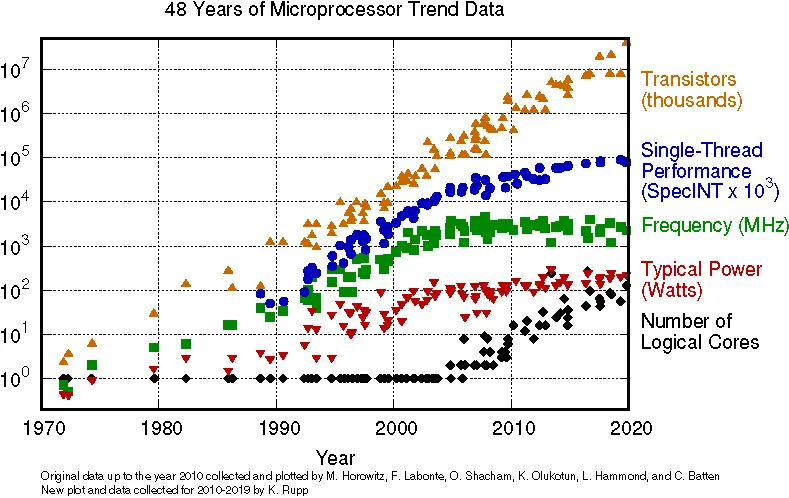
Re:Standard cells: Looking at individual gates in the Pentiu... by kragen on Monday July 08, 2024 @04:58AM (#40903774)
yeah, that plots single-threaded performance, not total compute power. the point it's making is that now those transistors are going to parallelism rather than to single-threaded performance, and also the compute power per transistor stopped increasing around 02007 with the end of dennard scaling

your problem doesn't have to be ep to scale to 10² cores

i suspect it's true that compute power per transistor is dropping because thermal limits require dark silicon, but that plot doesn't show it

Re:Standard cells: Looking at individual gates in the Pentiu... by caf on Sunday July 07, 2024 @08:49PM (#40901722)
As the article mentions, producing an optimal layout is an optimisation problem where the related decision problem is NP-complete. Even laying out standard cells has to be done using heuristic solutions - blowing up the size of the problem by going from cells to transistors just makes that worse.

The logic is built out of standard gates and logic blocks like flip-flops anyway, so the overhead of using standard cells that implement those building blocks likely isn't too great.

Re:Standard cells: Looking at individual gates in the Pentiu... by klyrs on Monday July 08, 2024 @03:08PM (#40908401)
This is more apocryphal than lore, but the understanding I've picked up from EE friends is that standard cells are used because they're proven to work in a given fab process. You don't want your layout software coming up with a trillion different gate prototypes in the midst of laying out your logic circuit!