ICs are manufactured on silicon disks called wafers. Discs have two sides, and traditionally, everything was done on top. We can now do power on the bottom. This makes things go faster and use less power:
* Power wires are big (and can be a bit crude). The bigger the better. Signal wires are small and precise. Smaller is generally better.
* Big wires, if near signal wires, can interfere with them working optimally (called "capacitance").
* Capacitance can slow down signals on the fine signal wires.
* Capacitance also increases power usage when ones become zeros and vice-versa on signal wires.
* Big wires also take up a lot of space.
* Putting them on the back of the wafer means that things can go faster and use less power, since you don't have big power wires near your fine signal wires.
* Putting them in back leaves a lot more space for things in front.
* Capacitance between power wires (which don't carry signal) actually helps deliver cleaner power too, which is a free bonus!
This is hard to do, since it means somehow routing power through the wafer. That's why we didn't do this before. You need very tiny wires through very tiny holes in locations very precisely aligned on both sides. Aligning things on the scale of nanometers is very, very hard.
How did I do?
However, something like an 80286 didn't even require a heatsink, while my 80486 had a dinky heat sink similar to what you might find on a modern motherboard chipset. At the same time, on a micron node, wires were huge. A few special cases aside (DEC Alpha comes to mind), power distribution didn't require anything special beyond what you'd see on your signal wires, and wasn't a major part of the interconnect space.
Mapping out to 2024:
1) Signal wires became smaller than ever.
2) Power density is higher than ever, requiring bigger power wires.
So there is a growing disparity between the needs of the two.
At the same time, there is continued progress in figuring out how to make through-wafer vias more practical (see https://en.wikipedia.org/wiki/Three-dimensional_integrated_c...).
I suspect in 2000, this would have been basically restricted to $$$$ military-grade special processes and similar types of very expensive applications. In 2024, this can be practically done for consumer devices. As costs go down, and utility goes up, at some point, the two cross, leading to practical devices.
I suspect a lot of this is driven by progress in imagers. There, the gains are huge. You want a top wafer which is as close as possible to 100% sensor, but you need non-sensor area if you want any kind of realtime processing, full frame readout (e.g. avoiding rolling shutter), or rapid readout (e.g. high framerate). The first time I saw 3D IC technology in mainstream consumer use were prosumer-/professional-grade Sony cameras.
I have strong fundamentals, but again, I stopped following this closely maybe 15 years ago, so much of the above is speculative.
"Better" is relative, the layout introduces more fabrication steps so it's only better if you actually get some benefit from it. Decades ago designs didn't require as much power or have as many transistors to wire so it wasn't an issue.
You might as well ask why, since we can do it now, Shockley didn't simply start at 3nm. It's all a very long road of individual process techniques.
> You need very tiny wires through very tiny holes in locations very precisely aligned on both sides.
Key word here is "both sides". It has challenges similar to solder reflow on double sided boards: you need to ensure that work done on the first side isn't ruined/ruining work on the second side.
https://semiwiki.com/semiconductor-services/techinsights/288... seems to be a good description.
"The challenges with BPR are that you need a low resistance and reliable metal line that does not contaminate the Front End Of Line (FEOL). BPR is inserted early in the process flow and must stand up to all the heat of the device formation steps."
Contamination = metals used musn't "poison" the front-side chemistry. So they end up using tungsten rather than the more usual aluminium. (Copper is forbidden for similar chemistry reasons)
It also (obviously) adds a bunch of processing steps, each of which adds to the cost, more so than putting the rails on the front side.
Do you need to align that precisely? Can't the power side have very large landing pads for the wires from the signal side to make it much easier?
Historically, everything was etched, grown, deposited, and sputtered on one side of the wafer. The rest of the wafer was mostly mechanical support. The other side of the wafer is a universe away.
The world is more complex today, but that's a good model to keep in mind.
For a 3d integrated circuit, you would do this, and then e.g. grind away the whole wafer, and be left with a few micron thick sheet of just the electronics, which you'd mechanically place on top of another similar sheet. That's every bit as complex as it sounds. That's why this was restricted to very high-end applications.
As for whether the wafer is a huge ground plane, that's complex too, since it depends on the top of the device and the IC:
* First, it's worth remembering a pure silicon crystal is an insulator. It's only when you dope it that it becomes a conductor. The wafer starts out undoped.
* Early ICs had the whole wafer doped, and the collector of all the NPN transistors was just the wafer. There, it was a ground plane.
* SOI processes deposit a layer of glass on top of the wafer, and everything else on the glass. There, the wafer is insulated from the circuit.
So all of this can very quickly go in many directions, depending on generation of technology and application.
I'm not sure this post is helpful, since it's a lot of complexity in an ELI5, so I'll do a TL;DR: It's complicated. (or: Ask your dad)
Even so, I oversimplified things a lot (a lot of the processes to leverage the silicon wafer, but some don't):
https://en.wikipedia.org/wiki/Silicon_on_insulator
One of the things to keep in mind is that a silicon wafer starts with a near-perfect silicon ingot crystal:
https://en.wikipedia.org/wiki/Monocrystalline_silicon
The level of purity and perfection there is a little bit crazy to conceive.
It's also worth noting how insanely tiny devices are. A virus is ≈100nm. DNA is 2nm diameter. We're at << 10nm for a device. That's really quite close to atomic-scale.
There are something like ≈100 billion transistors per IC for something like a high-end GPU, and a single failed transistor can destroy that fancy GPU. That's literally just a few atoms out-of-place or a few atoms of some pollutant.
The level of perfection needed is insane, and the processes which go into that are equally insane. We are making things on glass, but the glass has to be nearly perfect glass.
No, it can't thanks to this fancy marketing strategy where you sell faulty GPUs at lower price, as lower-tier model.
I thought it came from Reddit, which is about as far from ‘managerial’ as one can get.
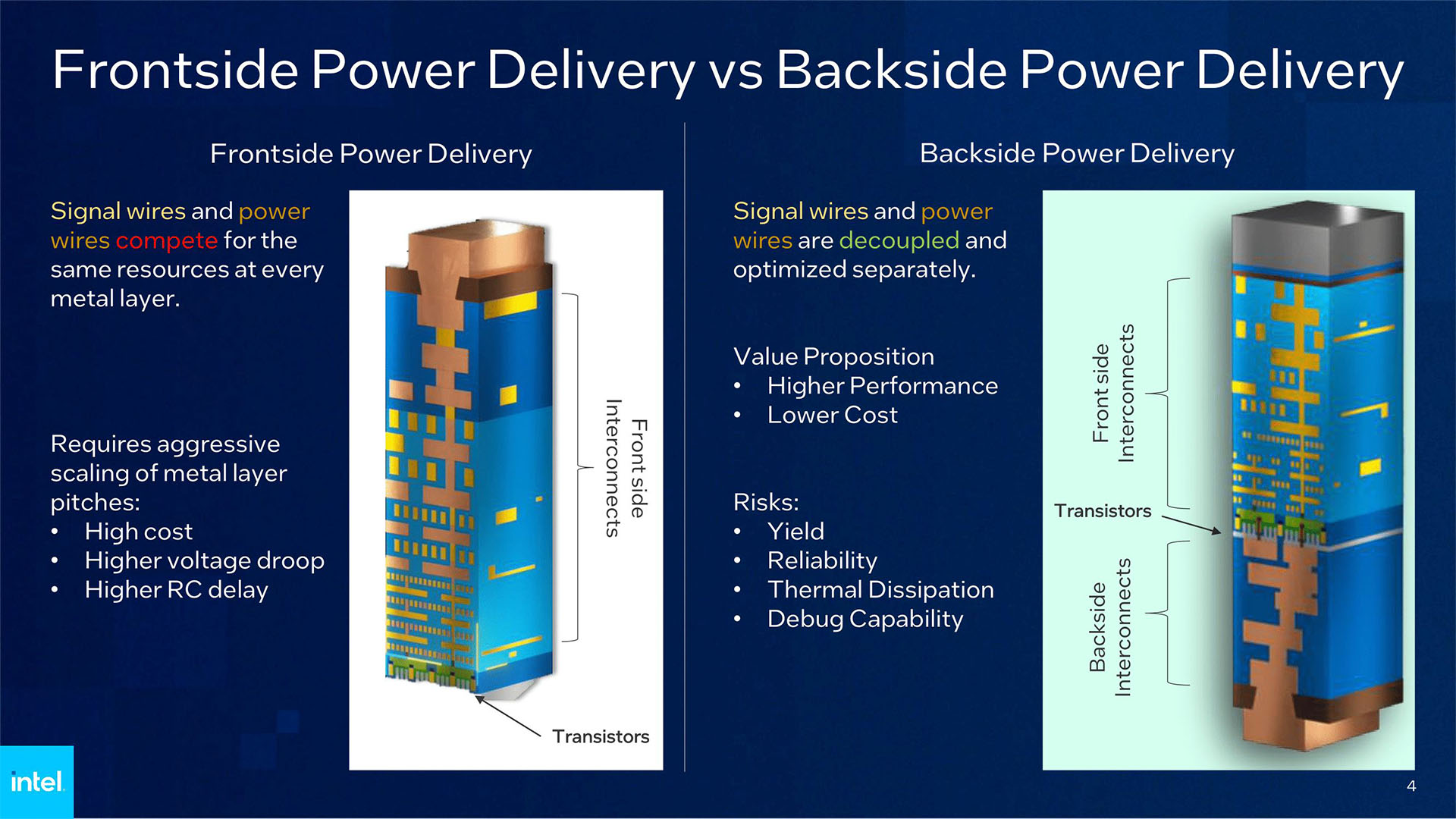
As a result, transistors are sandwiched between two wiring stacks. Resulting in lower noise, but makes heat removal a bit harder AFAICS.
See the image at: https://www.custompc.com/wp-content/sites/custompc/2023/06/I...
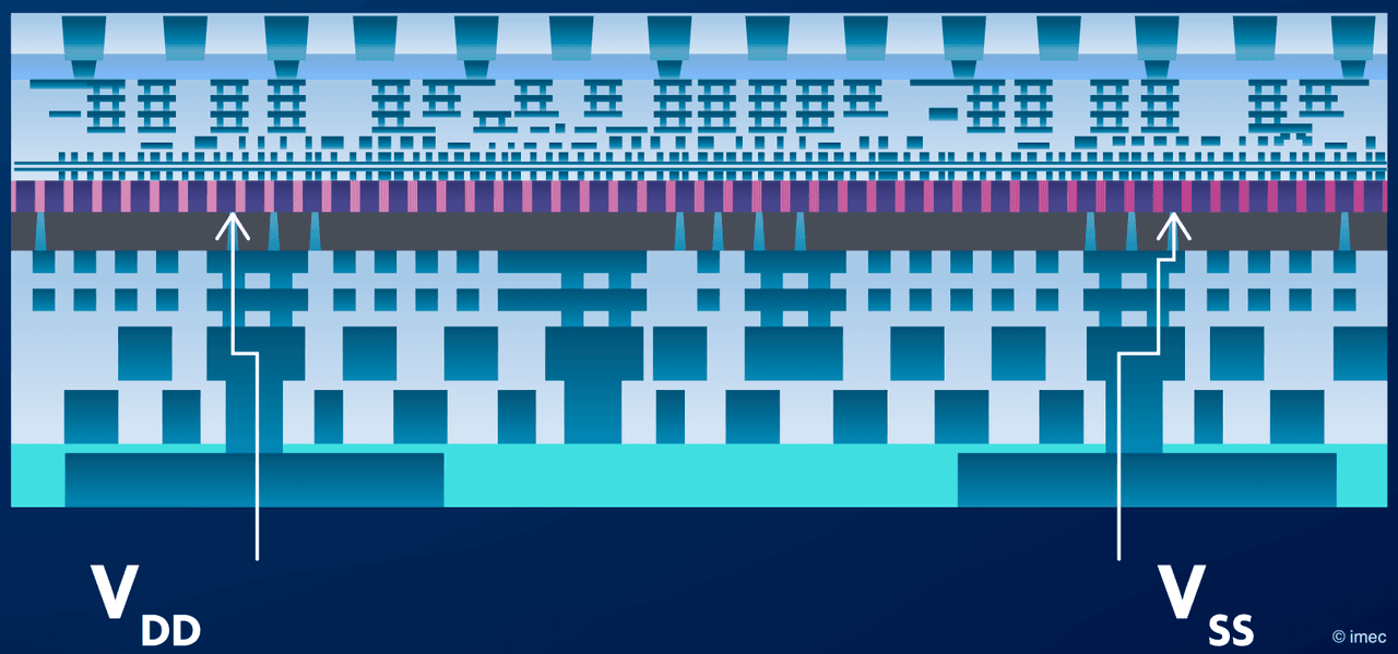
Are they sparse, like wires? Or solid, like the ground plane of a PCB? Are there "burried vias"?
frontside: https://www.imec-int.com/_next/image?url=%2Fsites%2Fdefault%...
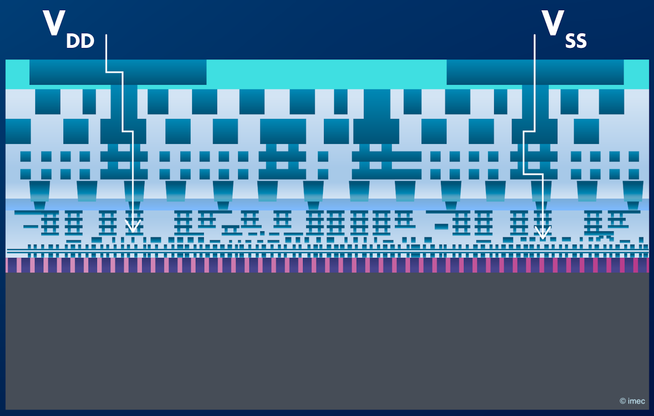
backside: https://www.imec-int.com/_next/image?url=%2Fsites%2Fdefault%...
Another graphic samsung used: https://www.thelec.net/news/photo/202210/4238_4577_1152.jpg

From https://www.tomshardware.com/pc-components/cpus/samsung-to-i...
> Typically, backside power delivery enables thicker, lower-resistance wires, which can deliver more power to enable higher performance and save power. Samsung's paper noted a 9.2% reduction in wiring length, enhancing performance
btw, you appear to be shadow banned, probably on account of being downvoted for making short comments like "good" or "I don't get it"
Short & simple responses may be adequate at times, but usually people will view it as not adding anything
Perhaps reviewing guidelines https://news.ycombinator.com/newsguidelines.html will give an idea of the ideal being yearned for (granted, it's an ideal). In general, trying to enhance the conversation with relevant information/ideas. "your links are 404" was definitely relevant here
I vouched for barfard's comment in this thread
More importantly, intel saw it as one of two key technologies of them moving into angstrom era, and was touting itself they'll be the first one to bring it to life (not sure they did).. so this seems to be more of a business power move.
more on all of it from anandtech: https://www.anandtech.com/show/18894/intel-details-powervia-...
It looks like the topology for backside moves the transistors to the middle so "singal wires and power wires are decoupled and optimized separately" instead of "compete[ing] for the same resources at every metal layer"
The very different requirements of the two is where a lot of the gains come in.
Precision is important. You'll notice every comment I made was as simple as I can make it, but /technically correct/. I did not oversimplify to where I changed facts.
* It's okay if five-year-olds don't fully understand something. That builds exposure, and leaves a placeholder for future information and curiosity.
* On the other hand, if you build out an array of misconceptions, those become very expensive to address later.
To a large extent, the younger the child, the more comfortable they will be with being told things they don't understand. A baby doesn't care if you're reading them a book on trucks or a book on homeomorphic transformations; they're picking out the phonemes. A toddler will trust you as an adult, and won't understand 90% of the stuff they hear anyways. A five-year-old, you can still say a lot they won't understand and they'll be not just okay but happy. By maybe seven, lack-of-understanding will become frustrating, and in most cases, by eleven, it's gone.
I could write a long essay on this stuff, and why it's so important to maintain that ability to be confused and half-understand, but I very intentionally leave placeholders when working with five-year-olds.