Re:LibrePCB – Create electronics the easy way
by Alupis on Thursday September 28, 2023 @06:03PM
(#37696476)
The main issue is the auto-router has no idea what any of the components are or what their requirements are. It just knows roughly physical dimensions and it's connected nets (traces between pins). These component requirements aren't something that can easily be "programmed" into the tool either - every component has it's own requirements, and they're not just electrical (such as needing certain amount of space around a component, or not placing next to other types of components, etc).
Without that knowledge, it's impossible to create a good auto-router/layout tool. The tools often just stack components as close together as physically allowed by the necessary traces.
For very trivial stuff, it might work ok. Anything else, no chance unfortunately.
Re:LibrePCB – Create electronics the easy way
by ShadowBanThis01 on Friday September 29, 2023 @01:44AM
(#37699718)
Yeah, that's too bad. With enough (in other words, complete) info, this seems like exactly the kind of thing computers should help us with.
Re:LibrePCB – Create electronics the easy way
by dbrgn on Thursday September 28, 2023 @06:24PM
(#37696686)
Ratsnest means that you have thin lines indicating which pads need to be connected. You can see them here: https://librepcb.org/features/board-editor/board-branching.g...
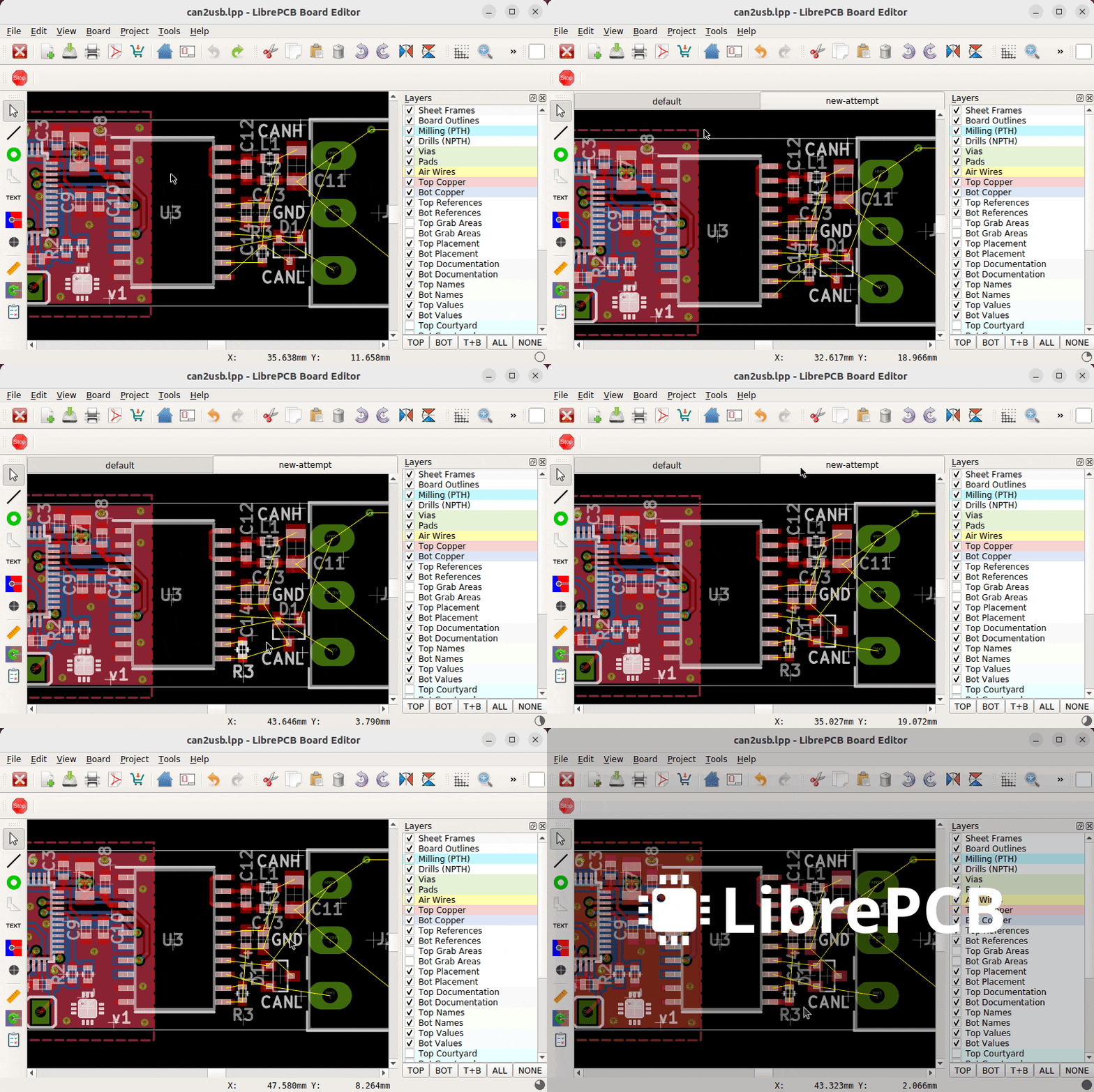
You start out the board deisgn by orienting your parts in a way that there are as few intersections as possible. Then you draw the connections, and the ratsnest lines disappear one by one. If you have intersections, you need to route around the part, or work with multiple PCB layers to get rid of them.
Re:LibrePCB – Create electronics the easy way
by civilitty on Thursday September 28, 2023 @07:14PM
(#37697199)
More representative sample of a ratsnest showing just a fraction of a board: https://cdn.vidyard.com/thumbnails/TdqAcWKgxGMwyKOQEtyTBg/26...
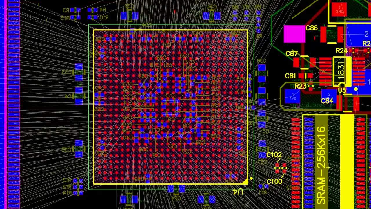
At that point "as few intersections as possible" becomes a bit of a lark and to maintain any semblence of sanity you have to prioritize connections, hiding all other nets.
Re:LibrePCB – Create electronics the easy way
by ShadowBanThis01 on Friday September 29, 2023 @02:15AM
(#37699904)
Thanks for the info.
Don't you think it'd be possible to create such a thing, which would also create labeled solder points for jumpers where traces needed to cross?
Maybe "rat's nest" already does this; I don't know what that is.