News for hackers. Stuff that matters.
Re:The legend of “x86 CPUs decode instructions into RISC for... by ant6n on Sunday June 18, 2023 @12:20PM (#36381621)
The decode with variable width instructions is one of the bottlenecks for ipc though. Its hard to imagine, for example, a 10-way decode on x86.

An internal fixed with encoding inside the instruction cache may work.

Re:The legend of “x86 CPUs decode instructions into RISC for... by ajross on Sunday June 18, 2023 @12:43PM (#36381851)
> Its hard to imagine, for example, a 10-way decode on x86.

Uh, why? Instructions start at byte boundaries. Say you want to decode an whole 64 byte cache line at once (probably 10-14 instructions on average). Thats... 64 parallel decode units. Seems extremely doable to me, given that "instruction decode" isn't even visible as a block on the enormous die shots anyway.

Obviously there's some cost there in terms of pipeline depth, but then again Sandy Bridge showed how to do caching at the uOp level to avoid that. Again, totally doable and a long-solved problem. The real reason that Intel doesn't do 10-wide decode is that it doesn't have 10 execution units to fill (itself because typical compiler-generated code can't exploit that kind of parallelism anyway).
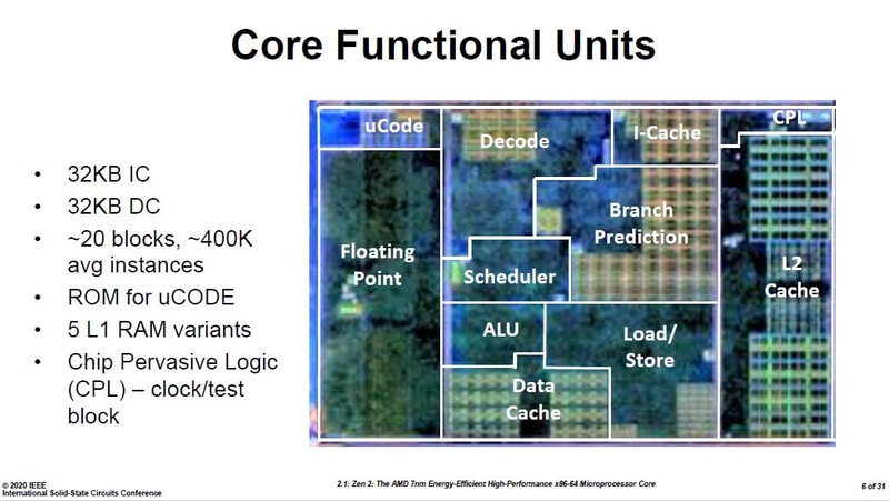
Re:The legend of “x86 CPUs decode instructions into RISC for... by formerly_proven on Sunday June 18, 2023 @12:56PM (#36381992)
That's a Zen 2 core: https://static.wixstatic.com/media/5017e5_bbd1e91507434d40bc...

Overlaid on a higher resolution die shot https://static.wixstatic.com/media/5017e5_982e0e47d7c04dd693...

Here's a POWER8 floorplan: https://cdn.wccftech.com/wp-content/uploads/2013/08/IBM-Powe... (The decoder is subsumed under IFU)

And POWER9 https://www.nextplatform.com/wp-content/uploads/2016/08/ibm-...
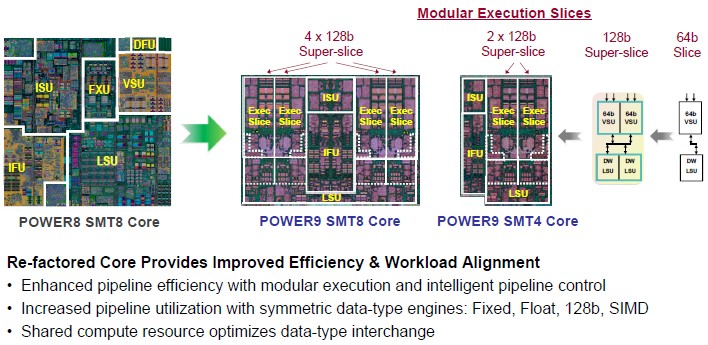
Didn't find any recent, reliable sources for Intel cores.

Re:The legend of “x86 CPUs decode instructions into RISC for... by hinkley on Sunday June 18, 2023 @02:10PM (#36382708)
Why does the middle of the Zen FPU look like cache lines?
Re:The legend of “x86 CPUs decode instructions into RISC for... by exmadscientist on Sunday June 18, 2023 @02:20PM (#36382823)
I believe those are the utterly massive register files needed to feed a modern vector FPU.
Re:The legend of “x86 CPUs decode instructions into RISC for... by hinkley on Sunday June 18, 2023 @02:47PM (#36383104)
That would have been my guess. But I don’t think I’ve ever seen a register file big enough that I could spot it without a label. I’m almost surprised they are so tall and not wide. Or is that because I am looking at it sideways, and each register is top to bottom?
Re:The legend of “x86 CPUs decode instructions into RISC for... by exmadscientist on Sunday June 18, 2023 @02:59PM (#36383204)
This is about Skylake rather than Zen2 but it's fascinating, if the subject of what's-really-in-a-register-file is fascinating to you: https://travisdowns.github.io/blog/2020/05/26/kreg2.html
Re:The legend of “x86 CPUs decode instructions into RISC for... by hinkley on Sunday June 18, 2023 @03:49PM (#36383760)
When I still read architecture docs like novels, there was a group experimenting with processor-in-memory architectures. Where the demo was Memory chips doing vector processing of data in parallel.

I wonder how wide SIMD has to get before you treat it like a CPU embedded into cache memory.

Though I guess we are already looking at SIMD instructions wider than a cache line…

Re:The legend of “x86 CPUs decode instructions into RISC for... by unnah on Monday June 19, 2023 @01:37AM (#36387661)
According to Agner Fog's manuals, the physical register file of a Zen 2 FPU contains 168 vector registers of 256 bits each. In total the vector registers hold 5 kB, so much less than the 32 kB L1 data cache, which isn't that large on the die image. Even if the middle of the FPU includes the register file, the regular structure must be mostly something else.
Re:The legend of “x86 CPUs decode instructions into RISC for... by formerly_proven on Monday June 19, 2023 @04:59AM (#36388829)
The register file allows much more accesses per cycle though and should actually be truly dual-ported (one register can be read and written in the same cycle). I'm not sure how exactly this works but Zen 2 has four vector units in the FPU so I'd naively expect the register file should be able to serve ~eight 256 bit reads per cycle and ~four 256 bit writes per cycle. So it should have those numbers of read and write ports at least? Additionally there should be a forwarding network around the ALUs. L1D only has a fraction of that connectivity. So between being dual-ported, having many more ports and probably the forwarding/bypass being integrated into this structure or at least being adjacent to it leads me to expect the FPU register file having a dramatically lower bit density than the L1D cache.