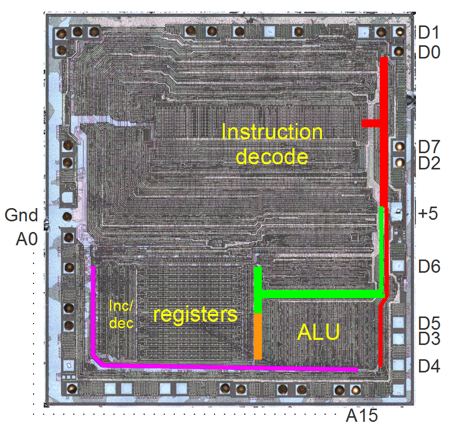
[1] http://static.righto.com/images/z80/z80_labeled_bus_addr.png
No, a PLA [1] and a microcode ROM are two very different animals.
A PLA is a way of compactly specifying combinatorial logic circuits (arrangements of and/or/etc. gates) and in the form that gave it the name, it is end user programmable (the P stands for Programmable). But at its heart, a PLA is just a big arrangement of logic gates. A signal goes in, and after the necessary gate delays settle, the result signal comes out.
Microcode is literally a "program" and is 'executed' in the same way that all other programs are executed, one instruction at a time, addressed by a program counter. There are also often branching instructions that generate new program counter values to use to sequence through the various steps. None of which exists in a PLA.
The appearance of similarity arises because both look similar in a silicon die photo (rows and columns of transistors), but they are very different and perform quite different functions on the chip.
Talking about the PLAs in these processors versus ucode ROM, the big difference is that in a PLA, typically several lines are enabled at a time. In contrast a ROM will only have one line active at a time with an address decoder sitting in front of it.
You absolutely could use a microcode ROM in the place of how these chips use their PLAs, it'd just take more die area.
You can see this logic/data equivalence in other places of hardware design too. For instance how FPGAs are a sea of SRAM, but are equivalent to standard cell chips. FPGAs are just slower, larger, and easier to modify.
I never said they were.
I said: "and in the form that gave it the name, it is end user programmable (the P stands for Programmable)" which is in the context of generic PLA's, not the specific PLA in a Z80 or 6502.
Technically a microcode ROM (or any ROM, really) is a (degenerate case of a) PLA. Hence the visual similarities, since that type of grid pattern will be observed with any PLA, whether ROM or general-logic.
I can imagine that some CPU designers from a particular world view (especially in the 70s) might only design in terms of microcode - but also design tools were pretty minimal, I can imagine that it might have been far easier to design things in terms of microcode rather than as PLAs - what you might be seeing here is the differences between different teams' in house custom tooling
Meanwhile the US4449184 patent [1] referenced in the post's footnotes has a lot of information about how the microcode works (and the meaning of the 21 instruction bits) and, in Tables 7-12, shows the microcode listings for some of the microcoded 8086 instructions.
However to be useful you need to know what each of those 21-bits is connected to, some will essentially be risc-like uCode instructions, the others will be tied to particular functions in the CPU or memory interface
There are two ways this is different from microcode. First, one instruction can trigger multiple "categories". Second, time is not an input here, so there is no stepping through operations.
The next part of the Z-80 instruction decoding is a big pile of AND-OR gates that generate the control signals based on the PLA outputs and the timing signals. For example, a gate might trigger the read-from-A-register signal for PLA-output-1 and time-1 or PLA-output-3 and time-1 or PLA output-1 and time-4. (These gates are all complex and were hand-drawn.)
The point of this is that both microcode and discrete logic generate particular control signals based on the instruction and time step, but they use very different ways to do this. With microcode, you can point to each micro-instruction as it executed, but in the Z-80, things are happening all over the place seemingly randomly.
Disclaimer: just a software engineer, I've only ever heard of microcode, never seen it or written it.
Hmm, the top part of the die shot looks like microcode to me:
http://visual6502.org/images/6502/6502_top_op10x_BF_4677.png