Once again, you are talking about an Intel CPU, so what you are saying makes no sense. It is not AMD's project. It is Intel's CPU that happens to use an AMD component.
The only EMIB in that product is between AMD's GPU and that GPU's DRAM; the Intel CPU die in that product is not using EMIB. The fact that the AMD GPU is using EMIB is significant—it's a somewhat external validation that EMIB has value as an alternative to conventional MCM packaging or large scale silicon interposers, both of which AMD uses for products of their own.
If EMIB wasn't saving money while offering sufficient performance, then Intel would have integrated the AMD GPU into this product using the off-the-shelf silicon interposers that AMD's own products use to connect the GPU to its HBM DRAM.
That is a nice claim, based on no evidence.
Intel spends billions subsidizing non-competitive products in order to try to build market share all the time. (mobile, ultrabook, etc, etc)
Unless you can present any evidence to the contrary (still no bandwidth numbers) it is just as likely that this product has EMIB because they couldn't get anyone else to use it and they need some shipping products with the tech to try and sell it.
The concept of market share does not apply to EMIB. It's an internal implementation detail, and Intel gains nothing from using EMIB in one of their own products over a cheaper solution that would still result in the end product being an Intel-branded part.
The only motivation that Intel could possibly have to use EMIB as any kind of loss-leader would be to entice third-party foundry customers to use Intel for the sake of EMIB. But attracting foundry customers is clearly not a priority for Intel, and Intel's primary goal with EMIB is to produce Intel products that may incorporate some third-party silicon, not to produce silicon to be incorporated into third-party products.
Correct. There's a conventional link through the package substrate carrying the PCIe signals from the CPU to the GPU. The only EMIB on that product is between the GPU and its DRAM. That's why the GPU and its DRAM are adjacent, while the CPU is about 1cm away from them: https://images.anandtech.com/doci/12003/intel-8th-gen-cpu-di...
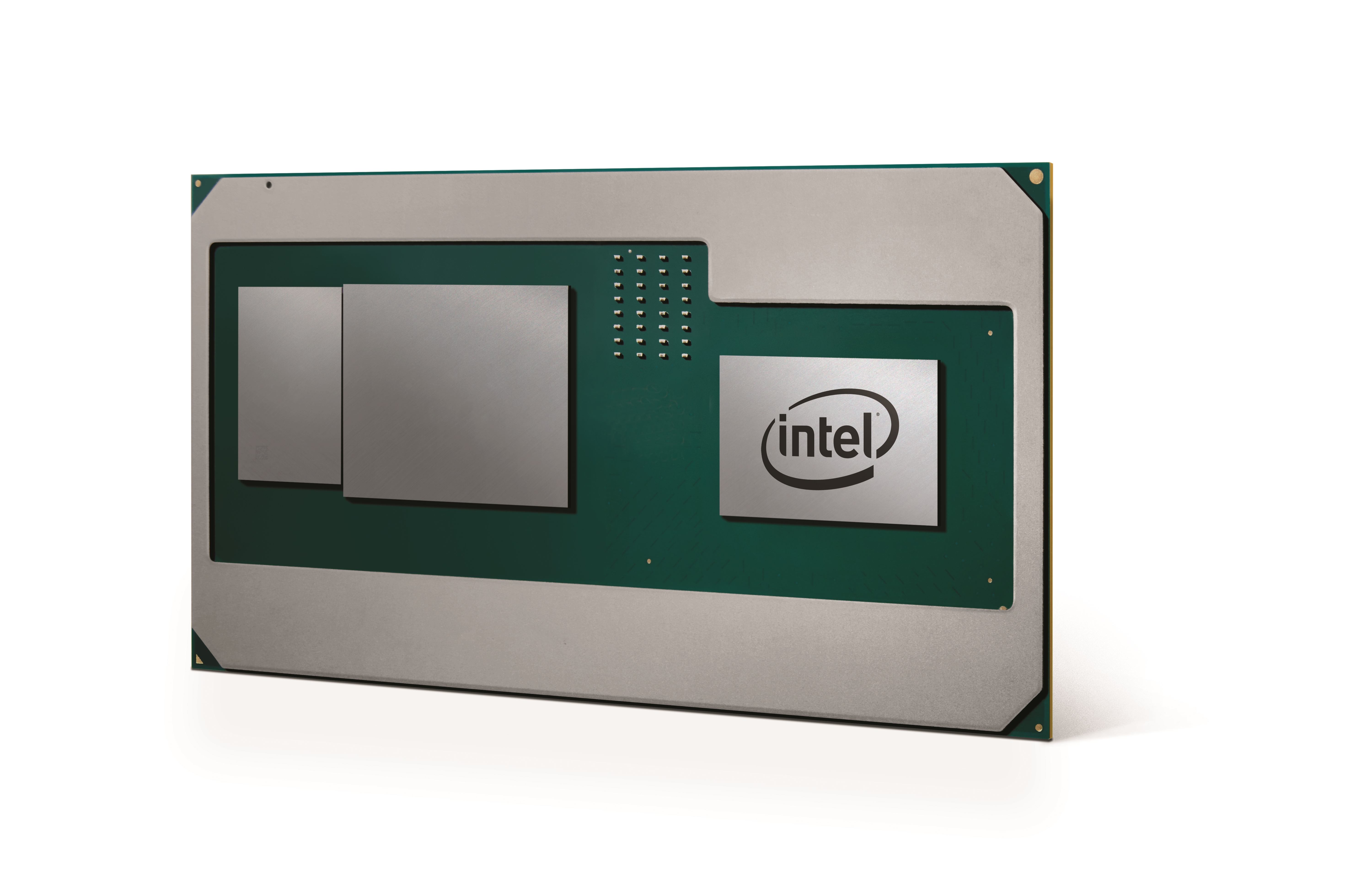
Intel would need to redesign the CPU die to accommodate an EMIB connection to the CPU. As it stands, an EMIB link would probably get in the way of lots of contacts that need to go to something other than the GPU, and EMIB wouldn't be worth the trouble for a relatively narrow and slow link like PCIe. The point of EMIB is to enable very wide and fast links between dies, so that inter-die communication is almost as fast as communication across a single die.
That article doesn't say EMIB is broken, it just says that the FPGA product Intel/Altera announced wasn't actually natively designed to use EMIB to interface with HBM. This is not relevant to a discussion of whether two Intel CPU dies could be connected over EMIB.
We do know that the Intel CPU with an AMD GPU on-package will have a much faster interconnect between the dGPU and its HBM2 over EMIB than AMD's EPYC and Threadrippper manage between CPU dies with a conventional MCM. It's also faster than Intel's old Crystalwell parts that used a conventional MCM to add an eDRAM L4 cache to a consumer CPU.
The limits of conventional MCM packaging are well-known across the industry and are a problem for everyone who's trying to use HBM-style DRAM or otherwise make high-speed inter-die links. Full-scale silicon interposers with TSVs are really expensive and would not have been adopted in high-end GPUs and FPGAs over the past several years if there was an alternative. Likewise, AMD wouldn't have adopted EMIB for their project with Intel if conventional MCM packaging were sufficient, because EMIB is still more expensive than not using two kinds of interconnects within the package.