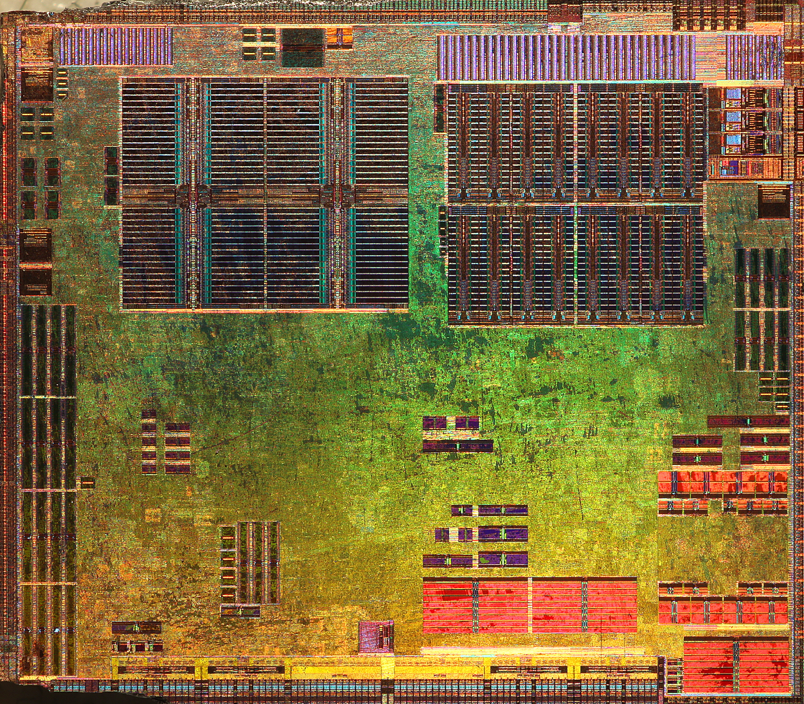
Re:5.5 mm in 1.25 nanoseconds
by bostonsre on Thursday January 13, 2022 @09:40AM
(#29921187)
Anyone know how much that would cost roughly? Wondering if they had a big reject bin that needed to be disposed of.
[ Parent
| on HN ]
Re:5.5 mm in 1.25 nanoseconds
by andreareina on Thursday January 13, 2022 @09:54AM
(#29921345)
Guessing that the cost for a wafer at a state-of-the-art process has gone up over the years but not that much, in the vicinity of ~$10,000?
https://twitter.com/chiakokhua/status/1306437988801486848 sourced from
https://cset.georgetown.edu/wp-content/uploads/AI-Chips%E2%8... p45
It depends, is the wafer passing or failing the manufacturing tests? This is an important consideration.
The manufacturing pipeline is generally pretty long too, and you can stop wafers midflight if you're just going to throw them out anyway. So for instance, if you have some B0 wafers that have enough metal layers that you couldn't easily change them into B1 wafers half way through the process, you might end up with it being cheaper to end up with unusable wafers for plaques and what have you. The fab is generally happy to have the extra capacity even for tail end of the design. There's generally some cheap customers that'll slot in wherever there's gaps.
Re:5.5 mm in 1.25 nanoseconds
by bowmessage on Thursday January 13, 2022 @12:19PM
(#29923508)
It was always rumored around the FAB that dropping a case of wafers was akin to totaling a Ferrari. Maybe ~20 wafers in a case, so this math checks out!
Pretty pricey for a plaque.. either they really liked him or they had some rejects I would guess.
They always have rejects. Actually, that's almost certainly an unfinished wafer. Modern flip chips don't look like that finished - you have an array of pads and power distribution covering all the cool features.
I think there's a good chance that wafer doesn't have any metal layers, or only M1 at most. It looks the same as the chips I've delayered and removed all or almost all of the metal layers from. For example, here's a shot of the Wii's GPU with the metal layers scraped off: