News for hackers. Stuff that matters.
Re:Designing Raspberry Pi 400 by geerlingguy on Wednesday November 04, 2020 @09:38AM (#24989393)
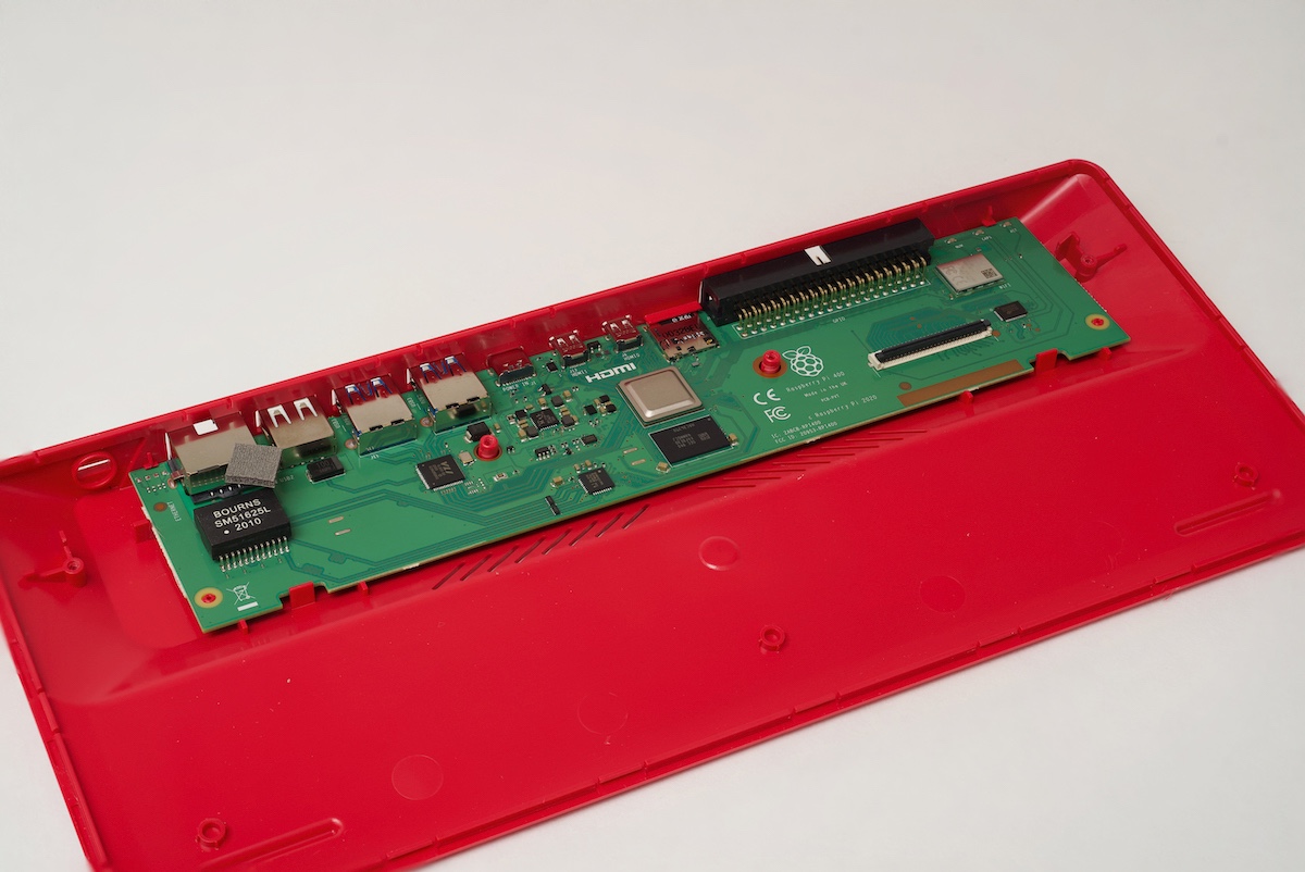
See this image from my tear down [1]: https://www.jeffgeerling.com/sites/default/files/images/4-pi...

You can see it's hard to find a good path from one side of the board (where the usb controller is located) to the other (where the HDMI ports are located) without using some vias or some crazy routing. The HDMI ports could be relocated probably but at the expense of more layers on the PCB (higher cost) or rotating the SoC, which would then necessitate even more of a redesign.

[1] https://www.jeffgeerling.com/blog/2020/raspberry-pi-400-tear...

Re:Designing Raspberry Pi 400 by cesarb on Wednesday November 04, 2020 @11:48AM (#24990657)
If you look closely at that image, and at the image of the other side of the board (https://www.jeffgeerling.com/sites/default/files/images/3-pi...), it's fascinating. The keyboard is USB 2 (as mentioned in the article, "one of the USB2.0 ports is dedicated to the keyboard") with its connector is on the right side, and the designer did find a good path from one side of the board to the other, using some crazy routing. It goes between the two USB 3 ports, and then below all the other ports until it reaches the right side, where it passes right next to the antenna and below the wireless chip to reach the keyboard connector. It's a tight fit, and there's no space for another pair.
Re:Designing Raspberry Pi 400 by a4444f on Wednesday November 04, 2020 @10:30AM (#24989865)
This seems to be an interesting and common problem (is there is a name for that?). If ribbons or additional pcbs are out of question, maybe a specialized / dedicated IC (I would describe its function as topological-only / electrically null) would work, I wonder if such ICs exist.
Re:Designing Raspberry Pi 400 by pjc50 on Wednesday November 04, 2020 @11:12AM (#24990300)
The two-pin version certainly exists and is sold as "zero ohm resistors" in surface mount packages. The multi-pin version probably exists but I can't find it with 30 seconds of searching.

But then there are two problems: controlled impedance and buried layers. Both the signals in question, HDMI and USB, are high-speed, and design recommendation will be that they cross as few vias as possible. They will be on "microstrip" paired line arrangements carried inside the board on one of the inner layers, while the top and bottom layers are ground planes. This won't be visible from a simple photograph of the board, you need an xray or the original Gerber files.

So while it's possible if you have enough space to punch a signal up to the surface of the board, through a package, and back down again in a different place, that will usually have an effect on signal integrity.

The normal solution is more layers. I don't know how many are there at the moment but I suspect it's 4. Increasing that to 6 costs more - not quite 50% more, but heading that way.