asdf_
The point of my previous comment is that it doesn't make sense to compare an entire TPU module (containing 4x TPUs) to a V100 board.
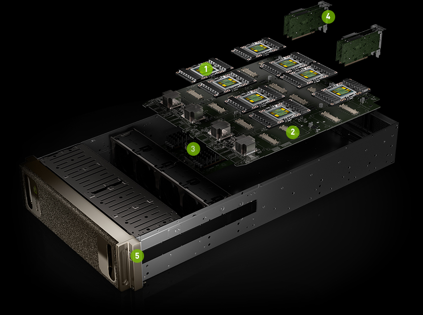
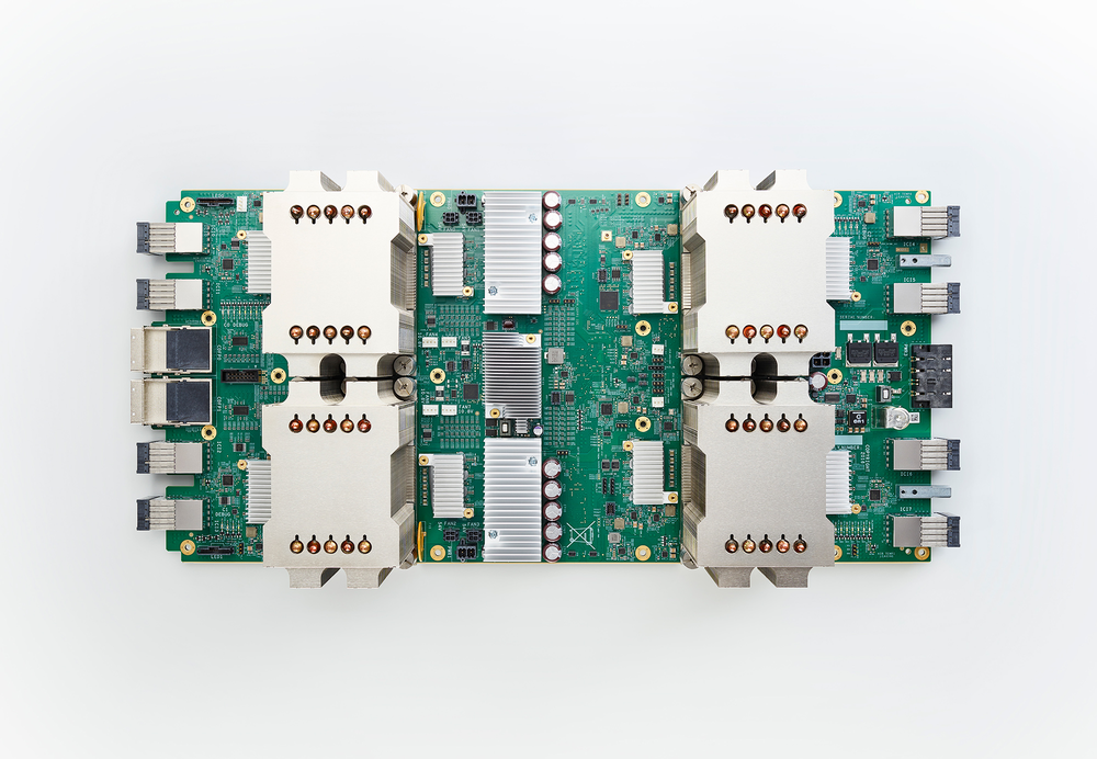
The closest comparison to a TPU module (with 4x TPUs) would be a dgx-1 board, which contains the nvlink bus that you mention, but also contains 8x V100 boards, hence why in my previous post I said you should compare the compute performance of a Volta DGX-1 (8x V100s) to 2 TPU modules (8x TPUs).
At the end of the day, it is simple, in a given area of space, you can get more compute performance from provisioning that area with V100s (in the form of using dgx-1s) versus provisioning it with TPUs (in the form of using TPU modules).
The closest comparison in terms of size would be 1 Volta DGX-1 (8x V100s) compared to 2 TPU modules (8x TPU2 chips).
Volta DGX-1: https://www.nvidia.com/content/dam/en-zz/Solutions/Data-Cent...
TPU Module: https://storage.googleapis.com/gweb-uniblog-publish-prod/ima...
And for completeness, this is the size of a single V100: https://cdn.arstechnica.net/wp-content/uploads/2017/05/34446...
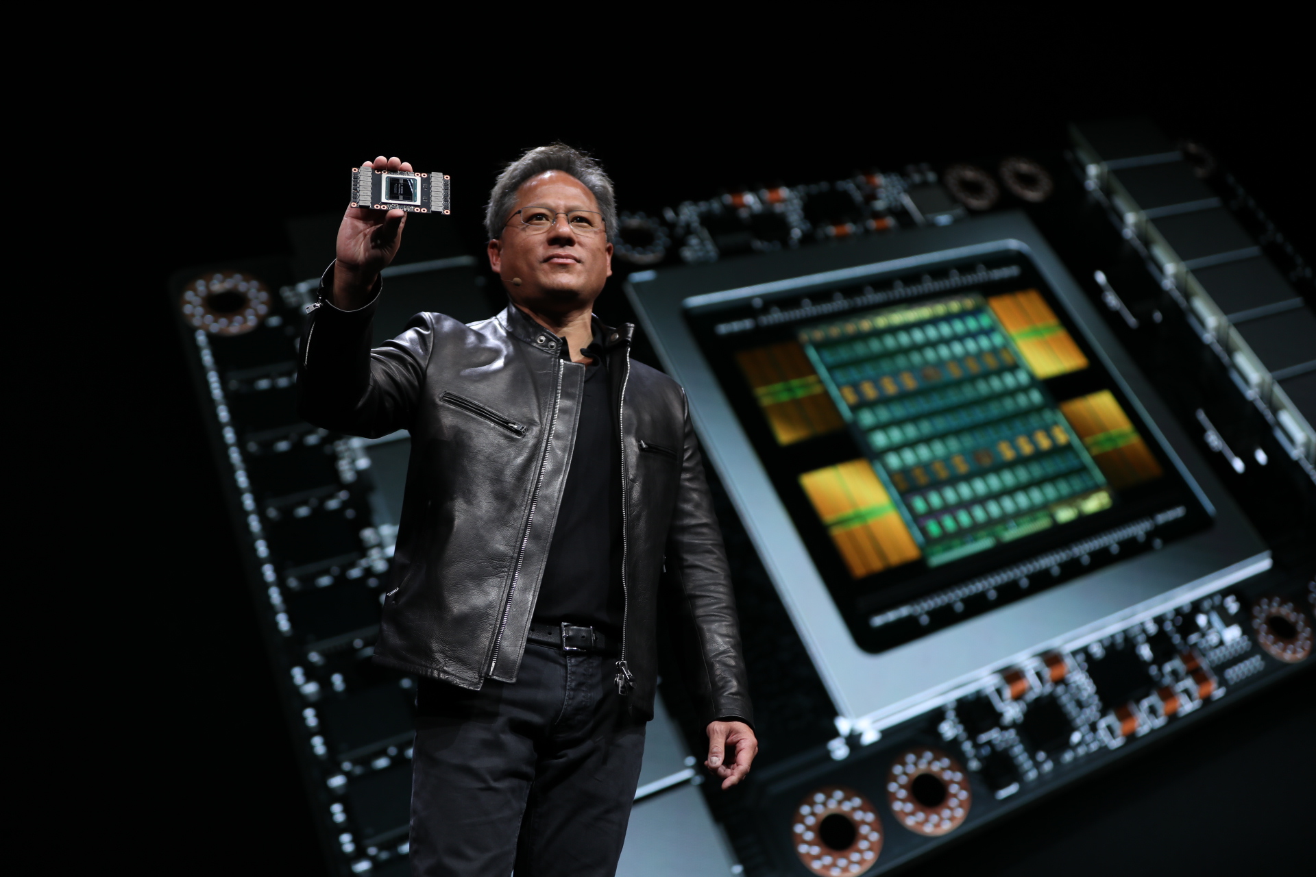
You can see that 8x V100s are still more computationally dense than 8x TPU2 chips. Density is a very important factor in datacenter design.
The closest comparison in terms of size would be 1 Volta DGX-1 (8x V100s) compared to 2 TPU modules (8x TPU2 chips).
Volta DGX-1: https://www.nvidia.com/content/dam/en-zz/Solutions/Data-Cent...
TPU Module: https://storage.googleapis.com/gweb-uniblog-publish-prod/ima...
And for completeness, this is the size of a single V100: https://cdn.arstechnica.net/wp-content/uploads/2017/05/34446...
You can see that 8x V100s are still more computationally dense than 8x TPU2 chips. Density is a very important factor in datacenter design.
V100 is 120 teraflops of tensor ops per chip: https://arstechnica.com/gadgets/2017/05/nvidia-tesla-v100-gp...